Numerical simulation of the magnetoresistance effect controlled by electric field in p–n junction
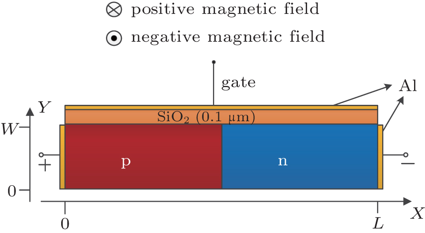
Schematic diagram of the p–n junction device, where the length

Numerical simulation of the magnetoresistance effect controlled by electric field in p–n junction |
Schematic diagram of the p–n junction device, where the length |
 |