


Van der Waals heterostructure of phosphorene and hexagonal boron nitride: First-principles modeling
[Zhang Peng, Wang Jing, Duan Xiang-Mei†,  ]
]
]
|
|


† Corresponding author. E-mail:
Projected supported by the National Natural Science Foundation of China (Grant No. 11574167), the New Century 151 Talents Project of Zhejiang Province,China, and the K. C. Wong Magna Foundation in Ningbo University, China.
We have studied the structural and electronic properties of a hybrid hexagonal boron nitride with phosphorene nanocomposite using ab initio density functional calculations. It is found that the interaction between the hexagonal boron nitride and phosphorene is dominated by the weak van der Waals interaction, with their own intrinsic electronic properties preserved. Furthermore, the band gap of the nanocomposite is dependent on the interfacial distance. Our results could shed light on the design of new devices based on van der Waals heterostructure.
Stimulated by the isolation of graphene from graphite, other two-dimensional (2D) layered materials with weak inter-layer van de Waals interaction (vdW), such as hexagonal boron nitride (h-BN) and phosphorene (P), were also isolated by liquid exfoliation routes[1] and the mechanical exfoliation method.[2,3] These 2D layered materials have attracted intensive research interest due to their fascinating electronic properties and extensive applications.[4–9] Among them, h-BN is an insulator with a large band gap,[10–12] which makes it difficult to tune the source–drain current using a gate voltage, therefore, h-BN has not yet been treated as a channel material in field-effect transistor (FET) fabrication. However, associated with its high purity, superior thermal and chemical stabilities, h-BN has emerged as a suitable dielectric to combine graphene or other graphene-like 2D crystal to create novel highly tailored heterostructures. For instance, Dean et al. reported that graphene devices on h-BN substrates have carrier mobilities and inhomogeneities that are almost an order of magnitude better than the devices on SiO2.[13] Theoretical studies have also shown the spontaneous opening and tuning of band structures of graphene on or between h-BN.[14,15]
Recently, a new 2D material, phosphorene, a single layer of black phosphorus (BP) patterned into a hexagonal puckered lattice,[16] has attracted considerable experimental and theoretical interest. Besides graphene, phosphorene is another stable elemental 2D monolayer which can be mechanically exfoliated experimentally.[3] Phosphorene has a unique band structure, its highly anisotropic effective masses and electronic properties can be tuned by strain and electrical field, leading to a sequence of transitions among direct semiconductor, indirect semiconductor, semimetal, and metal.[3,17–21] Moreover, this new layered material has a high charge-carrier mobility at room temperature[2,3] and a band gap that changes considerably as a function of the number of layers, going from 0.31 eV for the bulk black phosphorus to around 1.51 eV for a monolayer.[22]
Despite the promising physical properties explored in the phosphorene, it has been shown that the phosphorus suffers from oxidative degradation in the ambient conditions.[23] Thus, how to protect the phosphorene from degradation is a central research topic. Currently, vertical heterostructures based on 2D van der Waals materials have been considered as a novel way to construct devices that integrate the properties of their isolated components[24–27] with potential applications in optoelectronics[28–31] and nanoelectronics.[32,33] When two or more different 2D layered materials are assembled together, their properties may be preserved without any degradation. For example, a truly 2D nano-transistor has been constructed using heterostructures of graphene, h-BN, and MoS2, where graphene acts as both source or drain and gate electrodes, h-BN as the high-k dielectric, and MoS2 as the channel.[34] Several phosphorene based heterostructures have also been reported with diverse applications in more flexible ways, such as phosphorene/graphene,[27,35] phosphorene/MoS2,[32,36] and phosphorene/TiO2.[37] Very recently, BP/BN field effect transistors have been synthesized.[38] To the best of our knowledge, there is still a lack of systematic study of the effect of the BN monolayer capping on phosphorene.
In this paper, we choose the BN monolayer to protect phosphorene from degradation in the atmosphere and investigate the electronic properties of this hybrid nanocomposite. The results show that h-BN interacts weakly with the phosphorene via van der Waals interaction, both the properties of the phosphorene and BN are preserved in the nanocomposite. Moreover, interlayer interactions between the phosphorene and h-BN could induce tunable band gaps.
We perform first-principles study using state-of-the-art ab initio simulations, which are based on the density functional theory (DFT) as implemented in the VASP code.[39,40] The spin unrestricted generalized gradient approximation of Perdew–Burk–Ernzerhof (PBE)[41] and the projector augmented wave (PAW)[42] are adopted to treat the ion–electron interactions. The plane-wave cutoff energy for the wave function is set to 500 eV. The van der Waals-corrected function, optB88-vdW,[43,44] is used to account for the dispersion force between the atomic layers. OptB88-vdW has been demonstrated to reliably describe phosphorene systems[22,36,45] and BN systems.[46] The vacuum space in the z direction is about 15 Å to avoid the interaction between adjacent sheets due to the periodic image. During the geometric optimization, both lattice constants and atomic positions are relaxed until the residual forces on the atoms are smaller than 0.005 eV/Å and the total energy change is smaller than 1.0 × 10⁻⁵ eV. The GGA approach is well known to underestimate the band gap of semiconductors, the screened hybrid HSE06[47] method is also used to give the accurate band structures. To assess the stability of the heterostrcture, we calculate the binding energy Eb per P atom as follows:

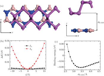
We construct a bilayer P/BN heterostructure by combining a 3 × 1 supercell of phosphorene with 12 P atoms and a 4 × 1 primitive orthorhombic cell of one BN layer with 8 B atoms and 8 N atoms. The optimized lattice constants of phosphorene are 3.30 Å and 4.62 Å along the x and y directions, respectively. For BN, the edge length of the basic hexagon is 2.51 Å. Since the electronic properties of phosphorene are sensitive to the strain,[19] we keep the phosphorene lattice fixed, and stretch the BN system to compensate the lattice mismatch. The supercell of the heterojunction is chosen to be 9.72 Å and 4.54 Å along the x and y directions, respectively. The same strategy was used in the previous studies for hybrid layers.[27] A lattice mismatch of around 3.3% compressive strain along the x direction and 4.4% tensile strain along the y direction occurs in BN, and no significant change is observed in its electronic structure. To obtain the equilibrium geometry, we optimize the composed structure using various starting positions of the phosphorene relative to the BN one. The stable configuration of P/BN stacked in the AB pattern is shown in Fig.
 | Fig. 1. (a) Top and side views of P on top of BN. The dark-magenta, light-pink, and blue balls represent phosphorus, boron, and nitrogen atoms, respectively. (b) Evolution of the total energy as a function of the displacement δ of the phosphorene layer relative to BN, taking the origin at the lowest energy configuration. (c) Binding energy as a function of the distance dP/BN. |
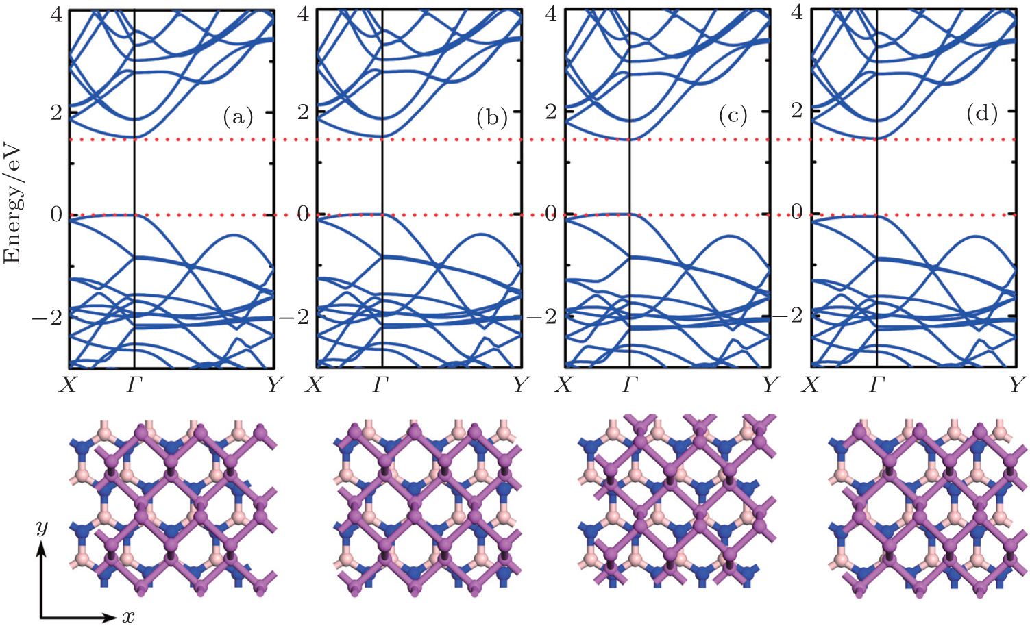 | Fig. 2. Band structures (upper panel) and atomic structures of P/BN (lower panel) for (a) equilibrium configuration; (b) δx = 0.5 Å; δy = 0.0 Å; (c) δx = −0.5 Å, δy = −0.5 Å; and (d) δx = 1.0 Å, δy = 0.0 Å. The red dashed lines are drawn as a guide with respect to the equilibrium configuration in panel (a). |
The binding energy of the junction is calculated to be 84 meV with an equilibrium distance of 3.49 Å, as shown in Fig.
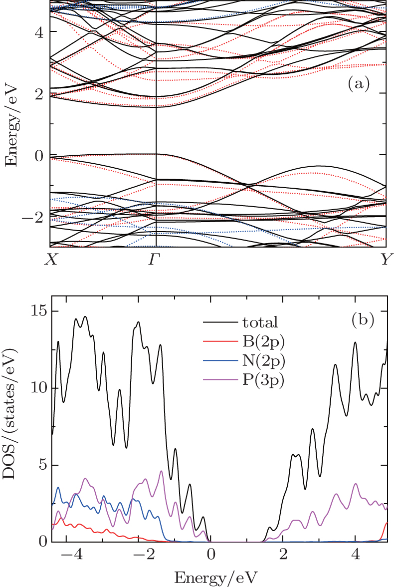 | Fig. 3. (a) Band structures of P/BN (black), pristine phosphorene (red), and BN monolayer (blue). (b) Projected density of states of P/BN heterostructure. |
We then analyze the charge transfer in the junction. Figure 
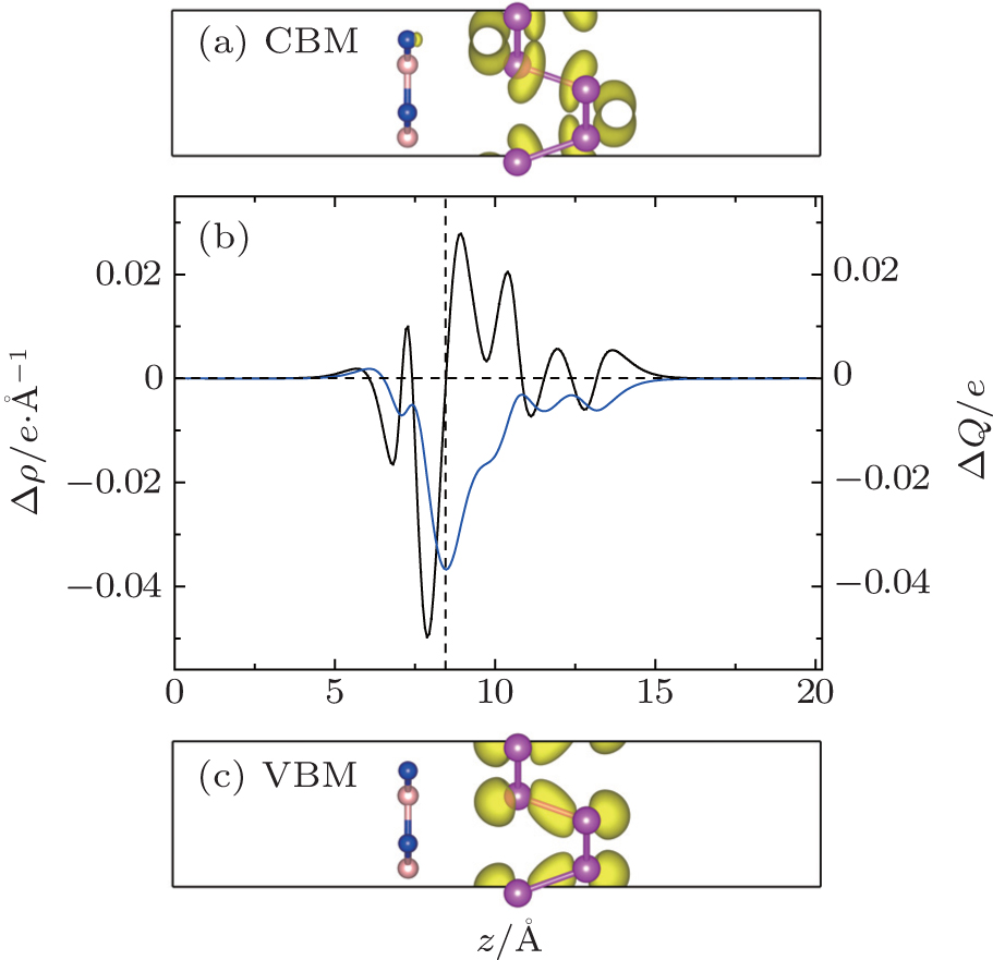 | Fig. 4. Decomposed charge distributions of (a) CBM and (c) VBM in the yz plane for the P/BN heterostructure. The yellow represents the charge distributions of CBM and VBM with an isovalue of 0.01 e/Å3. (b) Planar-averaged differential charge density δρ(z) (black) and the amount of transferred charge δQ(z) (blue) in the hybrid P/BN nanocomposite at equilibrium distance in the z direction. |
We reveal the tunable band gaps in P/BN by varying the interlayer distance, as plotted in Fig.
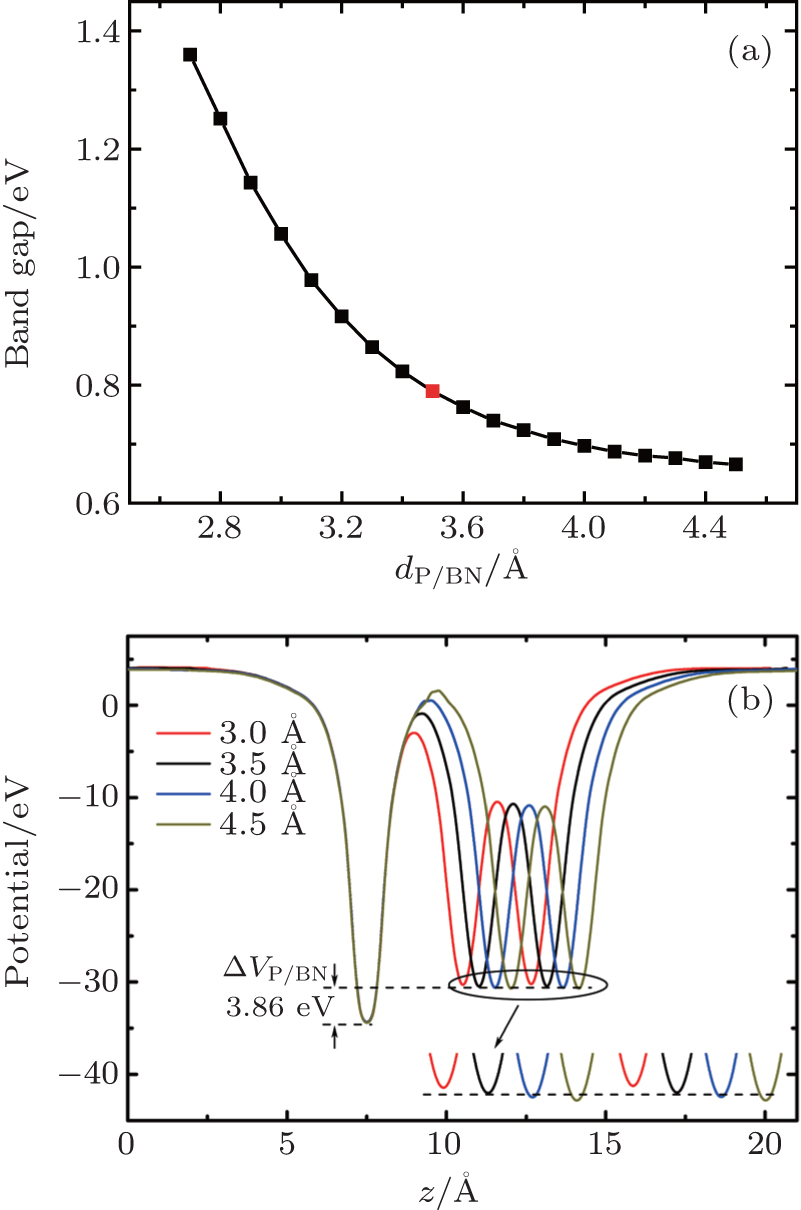 | Fig. 5. (a) The band gap of the P/BN heterostructure as a function of the interfacial distance. The BN layer is fixed and only the phosphorene layer is moved away from the BN layer. The red dot represents the equilibrium position. (b) Plane-averaged electrostatic potentials of P/BN at different interfacial distances dP/BN (Å). |
We have studied the structural and electronic properties of a hybrid P/BN nanocomposite using first-principles calculations. We show that the phosphorene interacts weakly with the BN sheet via weak vdW interaction which preserves their intrinsic electronic properties. Moreover, the variation of the interlayer distance could induce tunable band gaps in the hybrid P/BN nanocomposite. The redistribution of the electrostatic potential across the interface suggests that BN can serve as an active layer to tune the carrier dynamics of the phosphorene. With the excellent electronic properties superior to simplex BN and phosphorene monolayers, the 2D ultra-thin hybrid P/BN nanocomposite system is expected to possess great potential in new electronic devices.
| 1 | |
| 2 | |
| 3 | |
| 4 | |
| 5 | |
| 6 | |
| 7 | |
| 8 | |
| 9 | |
| 10 | |
| 11 | |
| 12 | |
| 13 | |
| 14 | |
| 15 | |
| 16 | |
| 17 | |
| 18 | |
| 19 | |
| 20 | |
| 21 | |
| 22 | |
| 23 | |
| 24 | |
| 25 | |
| 26 | |
| 27 | |
| 28 | |
| 29 | |
| 30 | |
| 31 | |
| 32 | |
| 33 | |
| 34 | |
| 35 | |
| 36 | |
| 37 | |
| 38 | |
| 39 | |
| 40 | |
| 41 | |
| 42 | |
| 43 | |
| 44 | |
| 45 | |
| 46 | |
| 47 | |
| 48 | |
| 49 | |
| 50 | |
| 51 |