Suppression of Andreev conductance in a topological insulator–superconductor nanostep junction
Zheng Yi-Jie, Song Jun-Tao, Li Yu-Xian†,
College of Physics & Information Engineering and Hebei Advanced Thin Films Laboratory, Hebei Normal University, Shijiazhuang 050024, China


† Corresponding author. E-mail: yxli@mail.hebtu.edu.cn

Project supported by the National Natural Science Foundation of China (Grant Nos. 11204065 and 11474085) and the Natural Science Foundation of Hebei Province, China (Grant Nos. A2013205168 and A2014205005).

Abstract
Abstract

When two three-dimensional topological insulators (TIs) are brought close to each other with their surfaces aligned, the surfaces form a line junction. Similarly, three TI surfaces, not lying in a single plane, can form an atomic-scale nanostep junction. In this paper, Andreev reflection in a TI–TI–superconductor nanostep junction is investigated theoretically. Because of the existence of edge states along each line junction, the conductance for a nanostep junction is suppressed. When the incident energy (ɛ) of an electron is larger than the superconductor gap (Δ), the Andreev conductance in a step junction is less than unity while for a plane junction it is unity. The Andreev conductance is found to depend on the height of the step junction. The Andreev conductance exhibits oscillatory behavior as a function of the junction height with the amplitude of the oscillations remaining unchanged when ɛ = 0, but decreasing for ɛ = Δ, which is different from the case of the plane junction. The height of the step is therefore an important parameter for Andreev reflection in nanostep junctions, and plays a role similar to that of the delta potential barrier in normal metal–superconductor plane junctions.

1. Introduction

Topological insulators (TIs) represent a new quantum state of matter.[1,2] With recent breakthroughs in two-dimensional (2D) and three-dimensional (3D) topological materials, a number of interesting and surprising phenomena have attracted much attention.[310] The electron velocity of the Dirac cone on the surface of a 3D TI[15], such as Bi2Te3 and Bi2Se3, depends on the properties of the material.[11,12] When two different 3D TIs are joined together, refraction phenomena due to the mismatch of electron velocities are expected at the junction,[13] and defects such as step-like imperfections may appear.[14] Quantum transport through a non-planar nanostep junction involving two different side surfaces of a 3D topological insulator has also been extensively investigated in recent years. In particular, it has been found that the conductance of a nanostep junction is suppressed in the large-energy limit by a factor of 1/3 as compared to the conductance of a similar junction between surfaces lying in a single plane.[15]

When one side of the nanostep junction is replaced with a superconductor (S), so-called Andreev reflection (AR) occurs due to the appearance of the superconducting energy gap Δ. For normal superconducting microconstriction contacts with a delta-function scattering potential at the N–S interface, the Andreev conductance amplitude is characterized by the parameter, Z, of the delta barrier.[16] In addition, it has been pointed out that for a ferromagnet–superconductor junction, the spin polarization of the conduction electrons in the ferromagnet can affect the AR.[17,18] At a normal-metal (ferromagnet)–superconductor interface in graphene, specular Andreev reflection appears.[1922] As for the nanostep junction, because of the different velocities of the Dirac fermions on either side of TI–TI junction, edge states appear along the step junction.[23] The velocity of the edge states is less than the velocities of the incoming plane waves, and the spins of the edge states have a nonzero component in the direction perpendicular to the surfaces.

Motivated by these novel phenomena,in this paper, we investigate Andreev reflection through a topological insulator-superconductor nanostep junction,consisting of a horizontal TI, a vertical TI, and a horizontal superconductor with emphasis on effects due to the step height.

2. Model and formulas

The model of the topological insulator–superconductor (N1N2S) step junction we have considered is shown in Fig. 1(a). The N1N2S junction, based on the 3D topological insulator Bi2Se3, has three regions: Regions I and II denote normally conducting topological-insulator surfaces, and region III is a topological-insulator surface with proximity-induced superconductivity produced by bringing the TI surface into contact with an s-wave superconductor. For convenience, we place the origin of the coordinate system such that x = 0 and z = 0 correspond to the interface between regions I and II with the orientation of the axes as shown in Fig. 1(a).

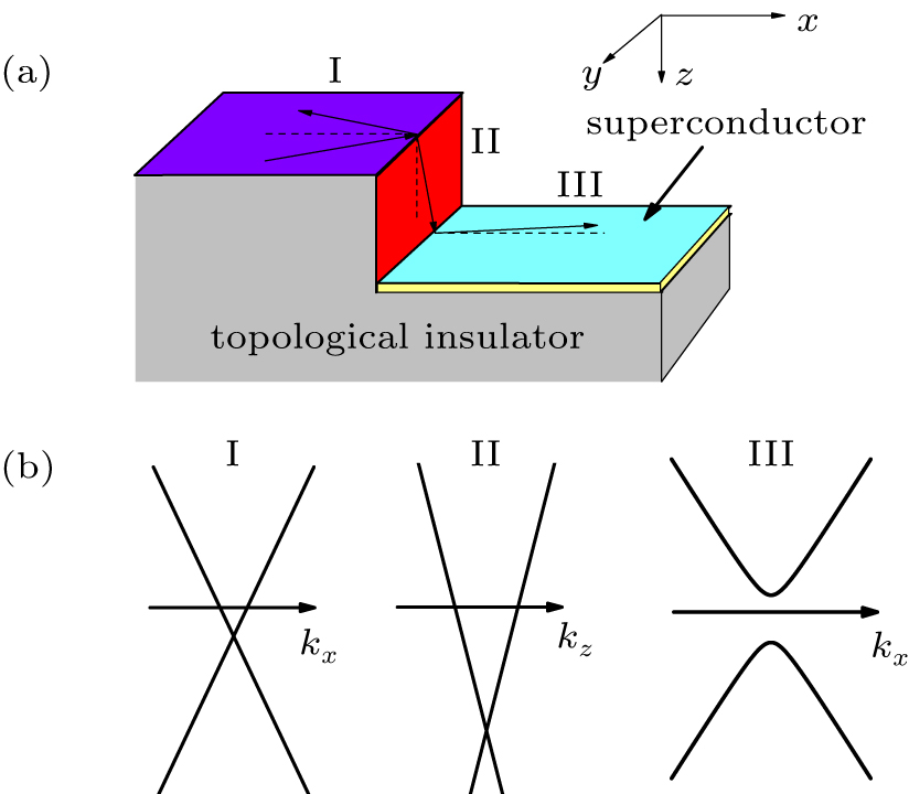
Fig. 1. (a) Schematics of the N1N2S step junction, the region I is in the xy plane, the region II yz plane, and the superconductivity region III in xy plane, respectively. (b) The energy dispersion in three regions, the propagating wave vector in regions I and III is kx and in region II is kz.

In region I, the effective surface Hamiltonian describing the carriers in the xy plane of the topological insulator is given by , where is the Dirac point energy, represents the Fermi velocity on the xy surface, and the σx,y,z denote the usual Pauli matrices.

Similarly, the carriers in the yz plane of the topological insulator in region II are described by the effective Hamiltonian , where , and The parameters A1, A2, B1, B2, C, D1, D2, and M can be determined by fitting the energy spectrum of the effective Hamiltonian[15,24] with that obtained from ab initio calculations.[7] The factor η in front of kz in Hyz can be written as η = A1/A2, where A1A2, because there exists an elliptical Dirac cone describing the excitations of the yz surface. The factor η indicates that the Fermi velocity along the y direction is different from the Fermi velocity along the z direction in the yz plane. However, the Dirac cone is circular on the xy surface due to the fact that the Fermi velocities along the x and y directions are identical.

Since superconductivity couples the electron and hole wave functions, the Hamiltonian for the surface states on the topological superconductor in region III acting on the Nambu basis Ψ = (ψe ↑,ψe ↓,ψh↓, − ψh↑) is given by

where represents the surface Hamiltonian in the xy plane; μ denotes the chemical potential; U, the electrostatic potential which can be adjusted independently by a gate or by doping, and Δ is the induced superconducting pairing gap at zero temperature. All of U, μ, and Δ are 2 × 2 matrices,

The eigenstates in region I can be written as

with the corresponding energy eigenvalues given by , and the incident angle, by θ = arctan(ky/kx). Here the +(−) labels on the wave functions indicate respectively right (left) traveling electrons and right (left) traveling holes in region I.

Analogously, in region II, the eigenstates for the electrons and holes are

with corresponding momenta in the direction

for the electrons and

for the holes. The angles of refraction of the electrons and holes are given by and , respectively. The +(−) labels on the wave functions indicate respectively downwards (upwards) traveling electrons and downwards (upwards) traveling holes in region II.

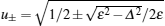
In the region III, the electron (hole)-like quasiparticles are both mixtures of electrons and holes, and the transmitted wave functions have the form of

where θ′ is the transmission angle, and Γ± = v±/u±, with , and .

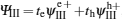
At each interface, we need to consider two kinds of scattering: (i) reflection as an electron and (ii) Andreev reflection as a hole. The total wave function in the different regions may then be written as , and , where the scattering coefficients re, rh, te, and th denote normal reflection, Andreev reflection, and transmission as electron-like and hole-like quasiparticles, respectively.

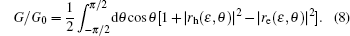
By taking into account the boundary conditions ΨI(x = 0) = ΨII(z = 0) and ΨII(z = L) = ΨIII(x = 0), the normalized Andreev conductance G/G0 at zero temperature can be calculated using the expression,

Here, denotes the normal density of states; W is the sample width, and the integration is over all angles of incidence, θ.

3. Results and discussion

In our calculations, typical parameter values for the 3D topological insulator Bi2Se3 were used: A1 = 2.2 eV·Å, A2 = 4.1 eV·Å,,,,, and Δ = 0.03 eV. For simplicity, we set the electrostatic potential to U = 0 eV and the chemical potential to μ = 0 eV in this paper.

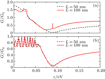
We first investigate the Andreev conductance as a function of the incident electron energy ɛ for different heights of the step (see Fig. 2). When the height is zero (L = 0), the nanostep junction becomes just a plane junction between a normal region and a superconducting region, and the Andreev conductance shows the expected behavior as a function of the incident energy, with G/G0 = 2 for ɛΔ and for ɛΔ. Eventually the conductance reaches G0 when ɛΔ.[16] When a real step is present, we can see from Fig. 2 that the effect of the junction height on the conductance is remarkable. For TIs with a step junction, the surfaces of the 3D TI lying in different planes have different electron and hole velocities, which results in the appearance of edge states propagating along the edge of the step. When the electrons tunnel through the step junction, unlike the case for the plane junction, the carriers have to transform their plane of propagation into that of region II. Consequently, some carriers are transmitted into edge states, and the Andreev conductance is suppressed. Figure 1(b) shows the energy spectrum for different regions. We can see that the Dirac point decreases in region II in which a top gate is applied to control the carriers. At the same time, the wave vector changes from kx to kz. Once the height of the junction is non-zero, even L = 1 nm, the shape of the conductance curve changes significantly. As the height increases, the Andreev reflection carriers repeatedly transmit and reflect through region II, and the conductance shows oscillatory behavior. With increasing energy, the oscillating amplitude of the conductance decreases gradually and then saturates at a value below unity at sufficiently large energy.

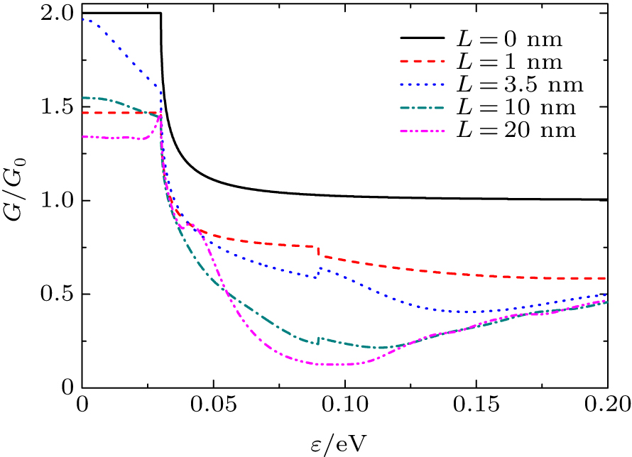
Fig. 2. The Andreev conductance in N1N2S junction as a function of incident energy ɛ with different junction height L.

We note that in Fig. 2 the conductance shows a sudden change at ɛ = 0.09 eV. This is because the Dirac point in region II for our model, , is 0.09 eV, but in region I, it is zero, and the electrons coming from region I tunnel through a potential barrier into region II. Consequently, the transmission coefficient shows a jump at ɛ = 0.09 eV. It may be seen, therefore, that the Dirac point energy affects the Andreev conductance.

The conductance for a relatively high N1N2S step junction is shown in Fig. 3(a). For comparison, the conductance through a normal metal TI nanostep junction N1N2N1 is also shown in Fig. 3(b). When the incident energy is larger than the superconductor gap, normal reflection is dominant and the Andreev reflection becomes weak. The two types of step junction have almost the same conductance curve shape for ɛ > Δ, and the conductance reaches a minimum at , arising from the mismatch of the electron velocities in the different planes. The conductances in the N1N2N1 step junction reach their minimums at the same value of ɛ for L = 50 nm and L = 100 nm. Similarly, when L = 50 nm, the conductance in the N1N2S step junction reaches its minimum at approximately the same value of ɛ. This case is also similar to the case shown in Fig. 2 for the larger values of L. However, for L = 100 nm, the minimum conductance occurs at a smaller incident energy, and there is a singular point at , which results from the Dirac point energy in region II. It may also be seen that the conductance in the N1N2N1 step junction oscillates and then saturates at 2G0/3 for large energies.[15] For the N1N2S step junction, at large energies, the conductance reaches a finite value which is larger than 2G0/3 due to the Andreev reflection.

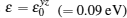
Fig. 3. (a) The Andreev conductance in N1N2S junction as a function of incident energy ɛ with different junction height L. (b) The normal conductance in normal step junction N1N2N1 as a function of incident energy ɛ with different junction height L.

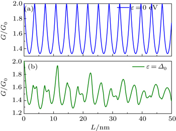
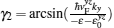
We next study the behavior of the conductance for two special values of the energy: ɛ = 0 and ɛ = Δ. For ɛ = 0, the analytical expressions for the scattering coefficients re and rh can be written as

The conductance as a function of the step junction height is plotted in Fig. 4(a) for the case of ɛ = 0. From Eqs. (9) and (10), it may be seen that the shape of the conductance curve is approximately that of a cosine curve. The electrons and holes transmit and reflect in region II, and the resonant condition arises due to quantum interference. As a function of the height L, the conductance oscillates, but the amplitude of the oscillation remains unchanged.

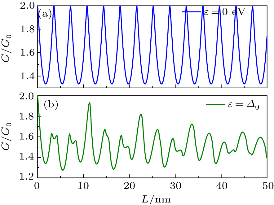
Fig. 4. The Andreev conductance in N1N2S junction as a function of the junction height L with different incident energies, (a) ɛ = 0 and (b) ɛ = Δ, respectively.

The Andreev conductance for ɛ = Δ is shown in Fig. 4(b). We can see from Fig. 4(b) that when L = 0, that is, the system does not have a step, the Andreev conductance is G = 2G0, which means that perfect Andreev reflection occurs in this plane junction. When the nanostep appears, the Andreev conductance oscillates as a function of the step junction height and the amplitude of the oscillation gradually decreases as the height L increases. The suppression of the Andreev conductance due to the presence of the step junction is clear. When the step height, L, is very large, the conductance fluctuates around the value G = 1.5G0.

4. Conclusion

In summary, we have studied Andreev reflection in a TI–TI–superconductor nanostep junction. Due to the edge states that lie along the boundaries between the different regions of the step junction, the conductance for a nanostep junction is suppressed. It is interesting to note that as a function of the step height the Andreev conductance presents an oscillatory behavior and that the amplitude of the conductance decreases when ɛ = Δ. However, for ɛ = 0 the amplitude of the oscillation does not change as a function of L, which is different from the case of a single planar junction. We hope that the suppression of the Andreev conductance discussed here can be measured using angle-resolved photoemission spectroscopy and/or electron tunneling with a STM tip placed close to the TI–S nanostep junction.

Reference
1Hasan M ZKane C L 2010 Rev. Mod. Phys. 82 3045
2Qi X LZhang S C 2011 Rev. Mod. Phys. 83 1057
3Hsieh DQian DWray LXia YHor Y SCava R JHasan M Z 2008 Nature 452 970
4Fu LKane C LMele E J 2007 Phys. Rev. Lett. 98 106803
5Kane C LMele E J 2005 Phys. Rev. Lett. 95 226801
6Kane C LMele E J 2005 Phys. Rev. Lett. 95 146802
7Zhang HLiu CQi XDai XFang ZZhang S C 2009 Nat. Phys. 5 438
8Bernevig B AHughes T LZhang S C 2006 Science 314 1757
9König MWiedmann SBrne CRoth ABuhmann HMolenkamp L WQi X LZhang S C 2007 Science 318 766
10König MBuhmann HMolenkamp L WHughes T LLiu C XQi X LZhang S C 2008 J. Phys. Soc. Jpn. 77 031007
11Xia YQian DHsieh DWray LPal ALin HBansil AGrauer DHor Y SCava R JHasan M Z 2009 Nat. Phys. 5 398
12Chen Y Let al. 2009 Science 325 178
13Takahashi RMurakami S 2011 Phys. Rev. Lett. 107 166805
14Alpichshev ZAnalytis J GChu J HFisher I RChen Y LShen Z XFang AKapitulnik A 2010 Phys. Rev. Lett. 104 016401
15Alos-Palop MTiwari R PBlaauboer M 2013 Phys. Rev. B 87 035432
16Blonder G ETinkham MKlapwijk T M 1982 Phys. Rev. B 25 4515
17de Jong M J MBeenakker C W J 1995 Phys. Rev. Lett. 74 1657
18Soulen R JByers J MOsofsky M SNadgorny BAmbrose TCheng S FBroussard P RTanaka C TNowak JMoodera J SBarry ACoey J M D 1998 Science 282 85
19Beenakker C W J 2006 Phys. Rev. Lett. 97 067007
20Zareyan MMohammadpour HMoghaddam A G 2008 Phys. Rev. B 78 193406
21Zhang QFu DWang BZhang RXing D Y 2008 Phys. Rev. Lett. 101 047005
22Schelter JTrauzettel BRecher P 2012 Phys. Rev. Lett. 108 106603
23Sen DDeb O 2012 Phys. Rev. B 85 245402
24Nussbaum JSchmidt T LBruder CTiwari R P 2014 Phys. Rev. B 90 045413