Tunable localized surface plasmon resonances in one-dimensional h-BN/graphene/h-BN quantum-well structure
[Zhang Kaibiao1, 2, Zhang Hong1, 3, 4, †,  , Cheng Xinlu1]
, Cheng Xinlu1]
|
|


† Corresponding author. E-mail:
Project supported by the National Natural Science Foundation of China (Grant Nos. 11474207 and 11374217) and the Scientific Research Fund of Sichuan University of Science and Engineering, China (Grant No. 2014PY07).
The graphene/hexagonal boron-nitride (h-BN) hybrid structure has emerged to extend the performance of graphene-based devices. Here, we investigate the tunable plasmon in one-dimensional h-BN/graphene/h-BN quantum-well structures. The analysis of optical response and field enhancement demonstrates that these systems exhibit a distinct quantum confinement effect for the collective oscillations. The intensity and frequency of the plasmon can be controlled by the barrier width and electrical doping. Moreover, the electron doping and the hole doping lead to very different results due to the asymmetric energy band. This graphene/h-BN hybrid structure may pave the way for future optoelectronic devices.
Graphene has emerged as a promising plasmonic material that combines the appealing optoelectronic properties with the ability of being tuned by chemical doping or electrostatic gating.[1–3] This allows for the realization of optical signal processors,[4] sensors, and light modulators.[5,6] To further enhance and extend the performance of these graphene-based devices, one of the challenges concerning this ultra-thin material is to enhance light-graphene coupling in a wide spectral range. Many discontinuous graphene structures have been designed to enhance the optical response associated with the excitation of graphene plasmon.[7–13] Instead of propagation, the plasmons in these patterned graphene arrays can be localized in a small region. These localized surface plasmons can significantly increase the light–matter interaction. Another new popular approach to extend its functionalities is plasmon hybridization due to the excellent compatibility of graphene.[14–17] In a hybrid structure, the resonant frequency can be tuned in a broader range.
Recently, graphene/hexagonal boron-nitride (h-BN) hybrid structures have been realized experimentally.[18–24] Ci et al. used a chemical vapor deposition (CVD) process to synthesize an atomic structure consisting of hybridized h-BN and graphene domains. This system exhibited a semiconducting behavior due to the carrier confinement within the graphene paths embedded in BN domains. Zhang et al. fabricated periodic graphene/h-BN heterostructures with precisely controlled domain sizes by using lithography patterning and sequential CVD grown step.[25] Theoretically, it has been predicted that one can manipulate the electronic band structure of graphene by doping with h-BN.[26–29] Band gap engineering plays an important role in applications of graphene. A minimal lattice mismatch allows graphene and h-BN to form a lateral planar heterostructure. Additionally, the large band gap difference between pure h-BN (∼ 5.9 eV) and graphene leads to distinct phase separation in the sheet of C and BN domains. Shinde et al. suggested that a zigzag BN chain on either side of a graphene nanoribbon may produce a major effect of quantum confinement. In this case, the BN domains act as infinite barriers due to the very large bandgap.[30] The charge carriers are confined within the graphene domain, which form a quasi-one-dimensional quantum well. Thus, the graphene plasmons in this heterostructure are expected to couple more strongly to their local environment.
In the present study, we numerically present a fully quantum-mechanical study of localized plasmon resonances in one-dimensional h-BN/graphene/h-BN quantum-well structures. The collective oscillations are mainly localized in the graphene domain due to the quantum confinement effect of the BN barrier. Compared with isolate graphene, the resonance absorption and the field enhancement exhibit a distinct strengthening in this hybrid structure. In addition, the intensity and frequency of the plasmon can be controlled by the barrier width and electrical doping, which provides the highly desirable feature of tunability to the plasmonic device. This study may provide a visible strategy for the well-ordered graphene/h-BN hybrid structure in the development of future devices.
The calculations have been performed using the real-space time-dependent density functional theory (TDDFT) approach as implemented in the OCTOPUS computer code.[31] TDDFT is a generalization of the static density functional theory to describe the electronic excitation and other time-dependent behaviors. This scheme offers a good compromise between computational cost and accuracy. In the previous works, it has been successfully used in predicting the absorption and plasmon resonances of nanostructures.[32–36] In the calculation, the inner shell electrons are treated by the Troullier–Martins norm-conserving pseudopotentials,[37] and the exchange and correlation interaction is included within the local-density approximation (LDA).[38] The linear response can be obtained by propagating the system with time-dependent Kohn–Sham equations under an impulse perturbation with a damping parameter of 0.15 a.u. Then the frequency-dependent absorption spectra are extracted by Fourier transform of the dipole strength. The simulation zone is a sphere around each atom with a radius of 6 Å and a uniform mesh grid of 0.3 Å. The Kohn–Shan wave functions are typically evolved for 6000 steps with a time step of Δt = 0.003 ħ/eV.
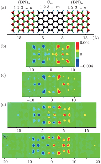
According to the experiment result,[18] it is more likely that graphene and h-BN domains could form a B–N–C configuration with N bonded to C atoms. The symmetrical one-dimensional quantum-well structures are constructed by integrating h-BN at the two sides of rectangular graphene flakes to form a seamless in-plane h-BN/graphene/h-BN structure, as depicted in Fig.
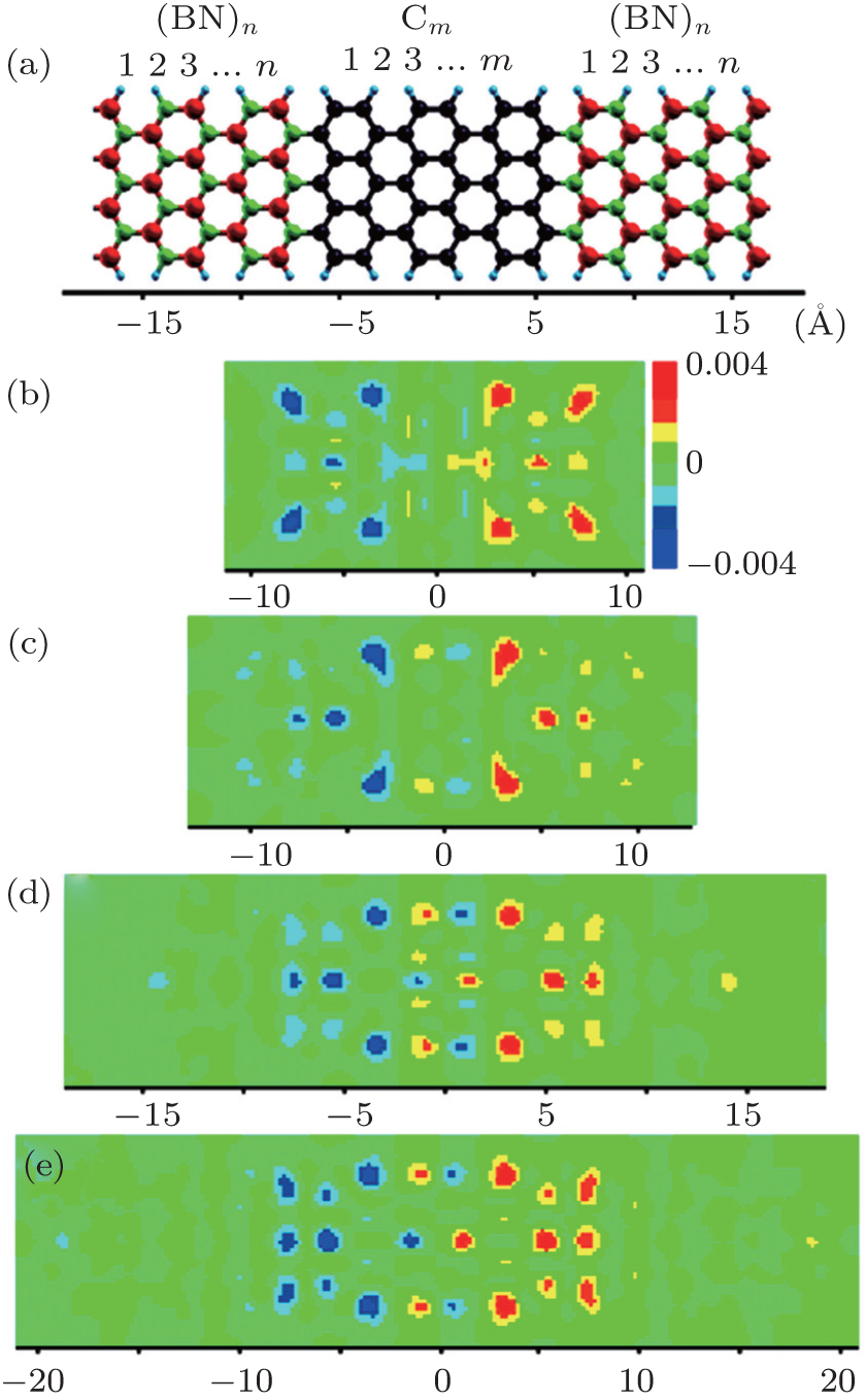 | Fig. 1. (a) Schematic of (BN)n/Cm/(BN)n quantum-well structure. Carbon, nitrogen, and boron atoms are represented by black, blue, and red balls, respectively. (b)–(e) The induced charge density distributions at the energy resonance point 0.72 eV for (b) (BN)1/C6/(BN)1, (c) (BN)2/C6/(BN)2, (d) (BN)4/C6/(BN)4, (e) (BN)6/C6/(BN)6. |
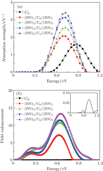
We first consider a series of 1D (BN)n/Cm/(BN)n quantum-well structures with fixed graphene length (m = 6) and varied BN length (n = 1, 2, 4, 6). The polarization direction of the impulse excitation light is maintained along the horizontal axis. Here, we focus on the optical response in the near-infrared region, aiming at a better understanding of the low-energy dipolar plasmon properties in these quantum-well structures. Figures
To gain more insight, we show the optical absorption spectra associated with these dipole oscillations in all the (BN)n/C6/(BN)n (n = 1, 2, 4, 6) systems in Fig.
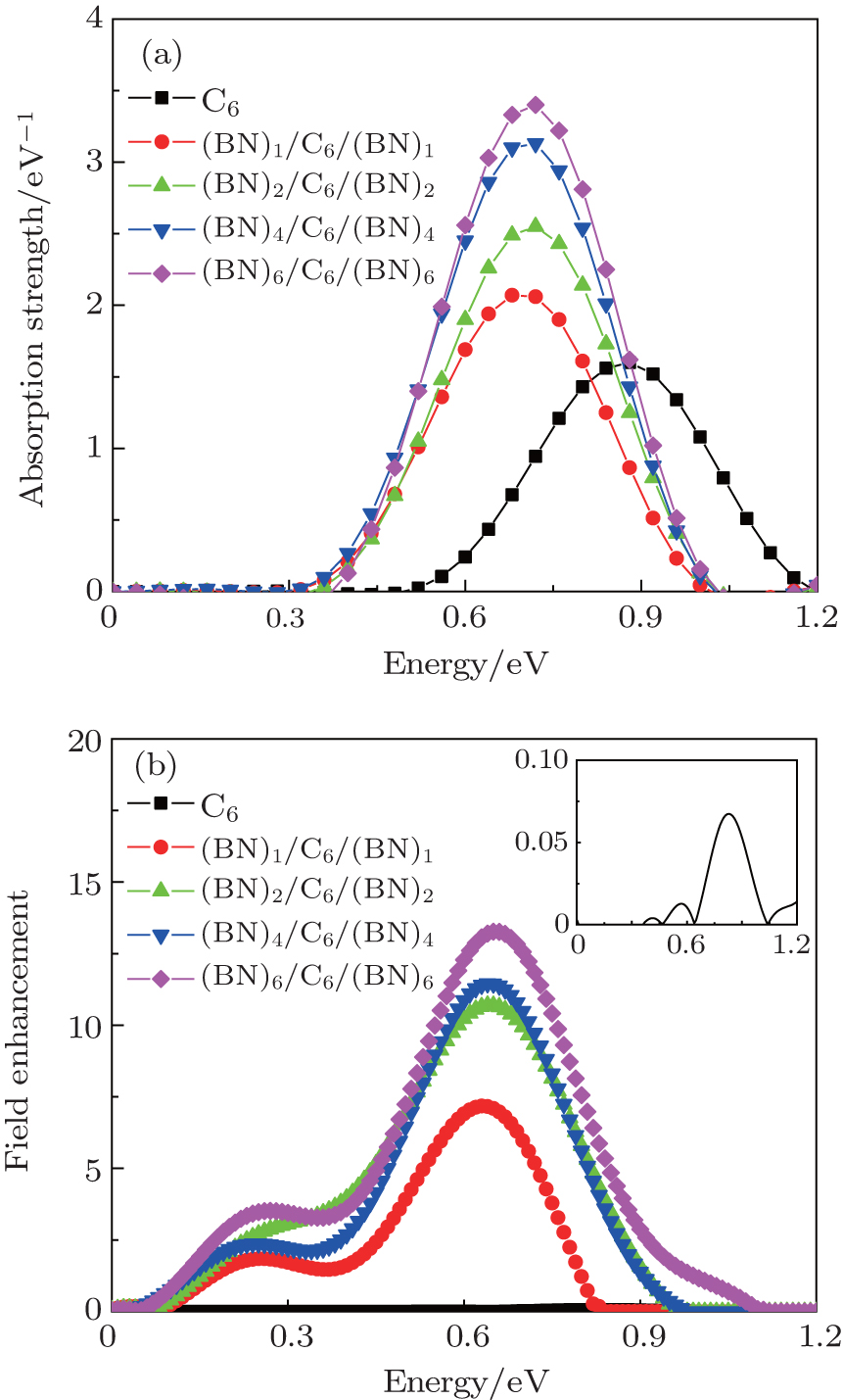 | Fig. 2. (a) Absorption spectra of a series of (BN)n/Cm/(BN)n quantum-well structures with fixed zigzag C chains (m = 6) and variable BN zigzag chains (n = 1, 2, 4, 6). (b) Energy-dependent field enhancement of graphene flakes in (BN)n/Cm/(BN)n. For comparison, the absorption spectrum and field enhancement (inset) of isolate graphene (C6) are also displayed. |
In general, the oscillating charge distribution is responsible for the large induced electric field enhancement. The field enhancement is obtained by deriving the effective potential.[40] Figure
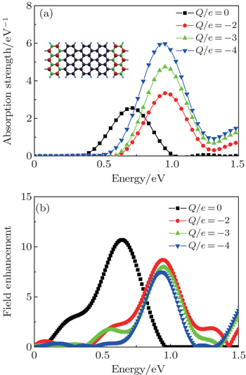
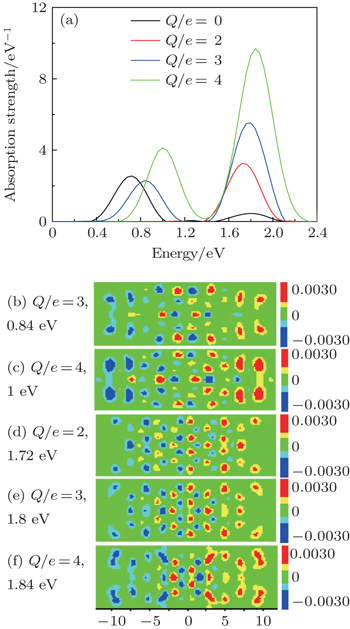
The electronic nature of plasmons suggests electrical tunability, which is convenient for integrable and high-speed modulation. Clear evidence has been obtained recently which demonstrates the ability to control the optical response in graphene by both electron and hole dopings.[41,42] However, these two dopings would lead to very different results due to the asymmetric energy band.[43,44] Here, the tunable plasmon properties can be obtained by adding or removing net electrons. A negative value means that we are adding electrons, while a positive value means removing electrons from the system. We first add electrons to the (BN)2/C6/(BN)2 quantum-well structure. Figure
 | Fig. 3. (a) Absorption spectra of (BN)2/C6/(BN)2 quantum-well structure as a function of net doped charge Q/e. (b) Energy-dependent field enhancement of graphene flakes in (BN)2/C6/(BN)2 structure as a function of net doped charge Q/e. |
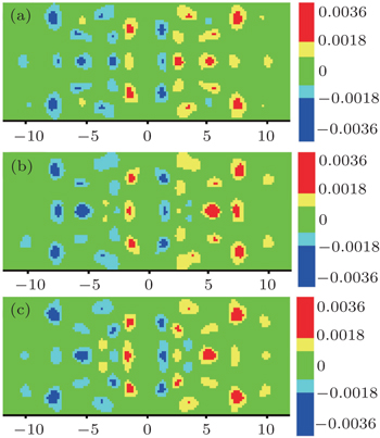
To elaborate the mechanism of field enhancement reduction, we show in Fig.
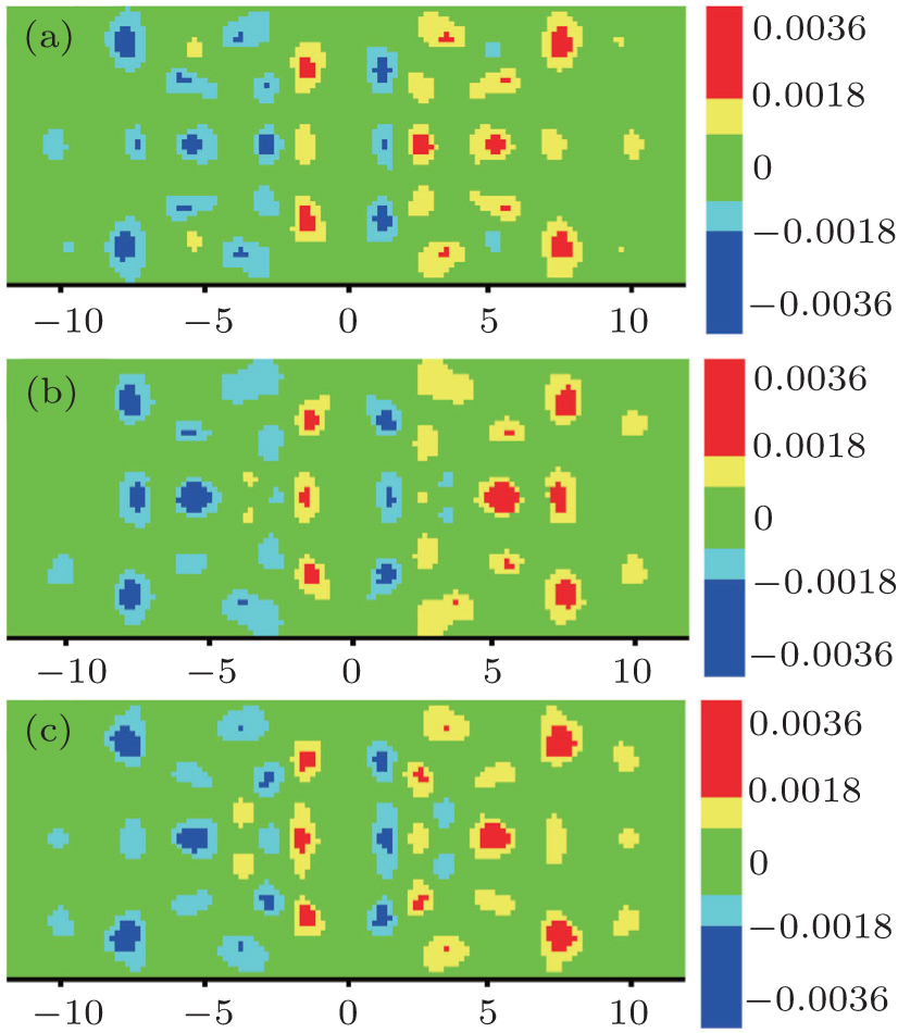 | Fig. 4. The induced charge density distributions of (BN)2/C6/(BN)2 with Q/e of (a) −2, (b) −3, and (c) −4. |
Then the hole doping is realized by removing electrons from the (BN)2/C6/(BN)2 quantum-well structure. The absorption spectrum displays a dramatic difference compared with that of electron doping, as shown in Fig.
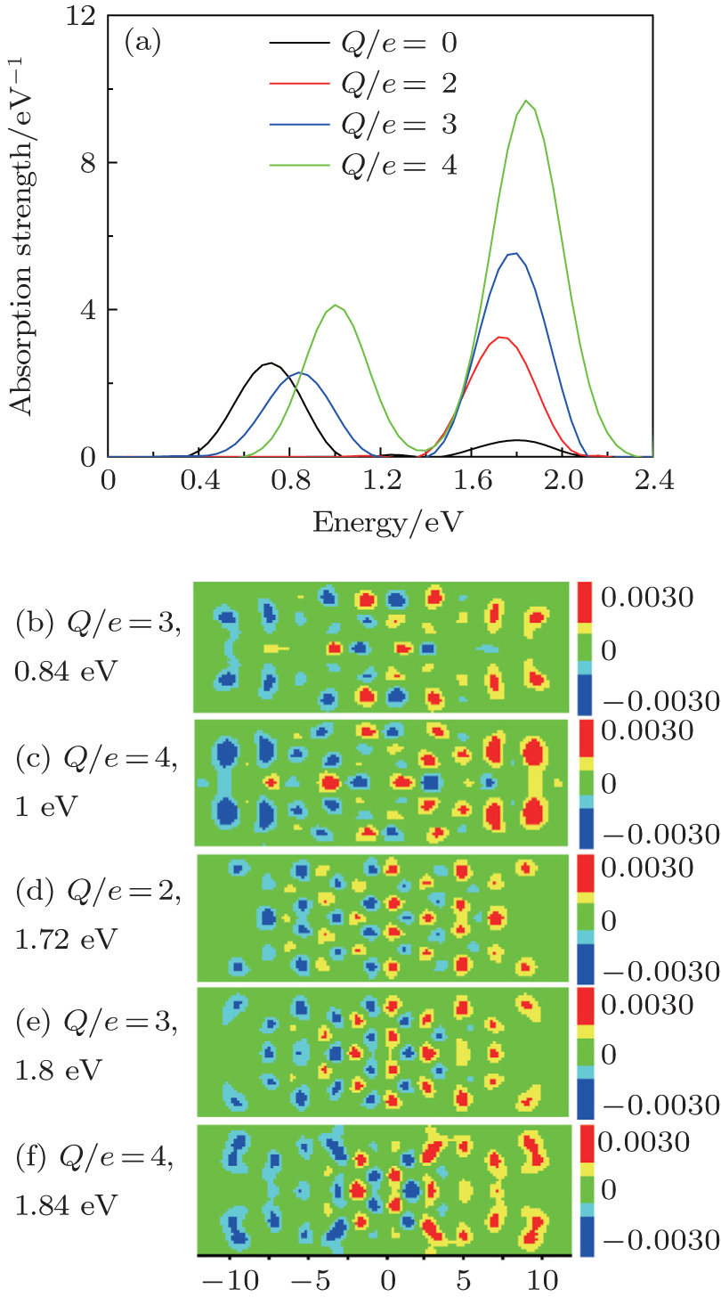 | Fig. 5. (a) Absorption spectra of (BN)2/C6/(BN)2 quantum-well structure as a function of net doped charge Q/e. (b)–(f) The induced charge density distributions of (BN)2/C6/(BN)2 with different net charge at the resonance energy point. |
To confirm this argument, we display in Figs.
We have investigated the tunable plasmon in 1D (BN)n/Cm/(BN)n quantum-well structures. The analysis of optical response and field enhancement demonstrate that these systems exhibit a distinct quantum confinement effect for the collective oscillations. Importantly, the plasmon in this structure can be sensitively tuned by electrostatic doping. The electron doping and hole doping lead to very different results due to the asymmetric energy band,[45] which lead to different confinement effects and different dipole–dipole interactions. This graphene/h-BN hybrid structure may pave a way for novel optoelectronic devices.
| 1 | |
| 2 | |
| 3 | |
| 4 | |
| 5 | |
| 6 | |
| 7 | |
| 8 | |
| 9 | |
| 10 | |
| 11 | |
| 12 | |
| 13 | |
| 14 | |
| 15 | |
| 16 | |
| 17 | |
| 18 | |
| 19 | |
| 20 | |
| 21 | |
| 22 | |
| 23 | |
| 24 | |
| 25 | |
| 26 | |
| 27 | |
| 28 | |
| 29 | |
| 30 | |
| 31 | |
| 32 | |
| 33 | |
| 34 | |
| 35 | |
| 36 | |
| 37 | |
| 38 | |
| 39 | |
| 40 | |
| 41 | |
| 42 | |
| 43 | |
| 44 | |
| 45 |