1. IntroductionSnO2/SnO is a wide direct-band gap (3.6 eV) semiconductor with high exciton binding energy (130 meV) at room temperature,[1] and also has an indirect band gap of about 2.6 eV.[2] It is a unique material of significant technological importance [3,4] and is used as transparent electrodes, solar cells, and solid-state gas sensors.[5–8] Under normal conditions, it exists in the form of a crystalline phase known as cassiterite. Another form of SnO2 with an orthorhombic structure is known to be stable only at high pressures and temperatures. The formation of orthorhombic phase SnO2 is intimately tied to a number of important synthesis parameters such as high pressure and temperature.[9,10] By using the pulsed laser deposition (PLD), we discover a simple way to fabricate the orthorhombic SnO2 thin film only by controlling the proper temperature and the ambient oxygen pressure during deposition.[11]
In this paper, we present our new successful fabrication of the orthorhombic tin oxide thin films with an indirect band gap (∼ 2.4 eV) by pulsed laser deposition at an oxygen partial pressure of 1 Pa and a substrate temperature of 450 °C. Under 1064-nm-wavelength pulsed laser irradiating on the sample at room temperature, a fast photovoltaic effect is observed in each of these films. The influence of oxygen vacancies on electrical properties is thought to originate from this photovoltaic effect. We also present the relations between the magnitude of photovoltage and power density of laser pulse and between the photovoltaic signals and laser positions on film. A possible detailed mechanism is put forward to explain this phenomenon. All data and analyses demonstrate that this orthorhombic tin oxide film with an indirect band gap may be a candidate for an infrared detector which can work at high pressures and temperatures.
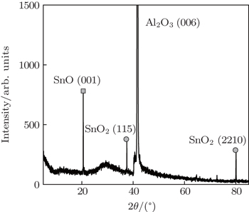
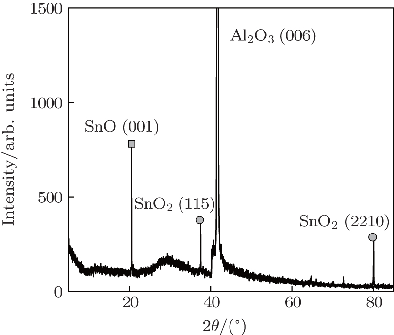
3. Results and discussionFigure 1 shows the XRD patterns of the prepared tin oxide thin film. Peaks appearing at 2θ = 37.56° and 80.08° correspond respectively to (1 1 5) and (2 2 10) directions of SnO2 structure, and the (0 0 6) direction of Al2O3 appears at 2θ = 41.73°. These reflections can be indexed with orthorhombic cell of SnO2. However, we also note that a peak centered around 2θ = 20.55° clearly belongs to the (0 0 1) direction of orthorhombic SnO structure. This indicates the lack of oxygen in the deposited film, which is known to originate from the surface layers of the SnO2 target during laser-induced oxygen desorption,[12] thereby leading to the growth of a nonstoichiometric compound.
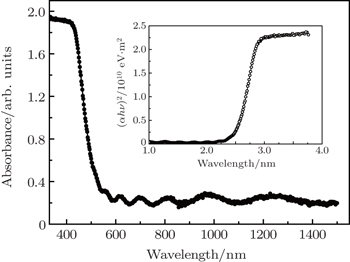
To investigate the band gap of tin oxide thin film, we carry out optical absorbance spectrum measurement at room temperature. Figure 2 presents the optical absorbance spectrum of tin oxide thin film corrected by the attenuation of a sapphire substrate. The absorption edge is located at a wavelength of about 500 nm. At the wavelengths of 600 nm, 700 nm, 800 nm, 100 nm, and 1200 nm, there are some wide and weak peaks due to the impurity energy levels. Under the assumption of the parabolic bands, the relation between α and Eg for an indirect transition can be written as

where
B is constant and the absorption coefficient is calculated from
α = 2.303
A/
t,
A being the absorbance and
t the film thickness. We also plot
α1/2 versus
hν for tin oxide thin film (shown in the inset of Fig.
2) and look for the best linear fit region at the band edge from which band gap (
Eg = 2.4 eV) is estimated from the intercept in the
hν axis.
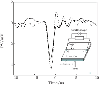
Typical ultrafast photovoltaic curves (solid and short dash dotted) for the photovoltaic signals are shown in Fig. 3 when the laser pulse was irradiated on the tin oxide surface (short dash dotted curve) and substrate (solid curve) respectively. The schematic of the experimental set-up for the photovoltage between two electrodes is shown in the inset of Fig. 3. The rising time of the photovoltaic signal is about 2 ns, which approaches to the maximum of the resolution of the oscilloscope. As the film is isotropic, the orientations of photovoltaic signals are the same when the laser irradiates on the film surface and the substrate. Owing to the scattering of the substrate, the peak value of photovoltage with the laser illumination on the tin oxide surface is bigger than that on the substrate at the same laser intensity. The photon energy of the laser pulse with a wavelength of 1064 nm (1.2 eV) is below the band gap (2.4 eV) of tin oxide. But due to the oxygen vacancy energy level and other impurity energy levels, the oxygen surface vacancy energy level is about 1.4 eV above the valence band edge at 100°.[13] We also find that there is a wide and weak peak at a wavelength of about 1000 nm in Fig. 2. This reveals that the tin oxide thin film can absorb the infrared light. So when the film is partially illuminated by the infrared laser beam, the valence electrons will transfer from the valence band to the impurity energy levels, then jumping into the conduction band and becoming free electrons. The holes will be generated in the valence band correspondingly. A carrier gradient will form between the illuminated and the nonilluminated areas. As the carrier mobility in the illuminated zone is much higher, electrons will flow from the illuminated zone to the non-illuminated region. At the same time, a transient field and also photovoltage are therefore built up.
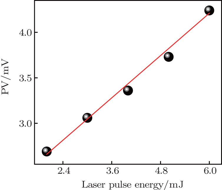
The peak value of the photovoltaic response as a function of power density is plotted in Fig. 4. It is found that the value increases linearly with laser pulsed energy increasing in a range from 2 mJ to 6 mJ. This may be caused by separation of deep-level impurities and the release of electrons in a deeper part of the film due to the temperature increasing as the laser energy intensity increases. And the hopping transport of carriers, which is common in disorder semiconductors like amorphous Si and organic semiconductors[14] is also another contributor to this linearly increasing peak value.
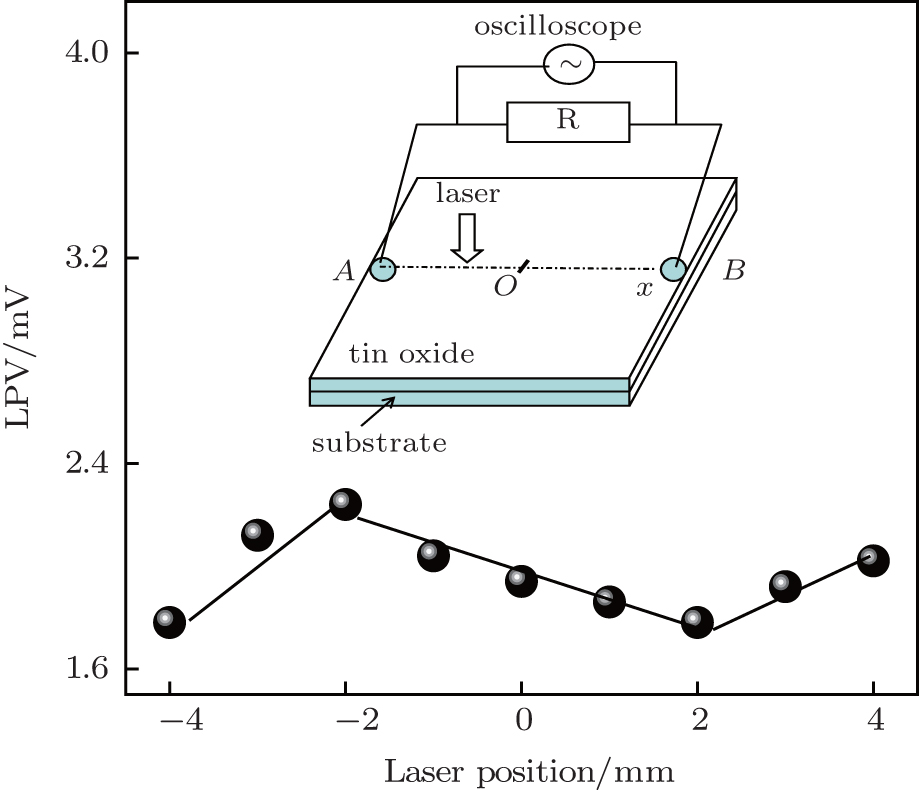
In Fig. 5, the pulsed laser beam with an energy density of 0.05 mJ/mm2 passes through a 1-mm-diameter aperture. The inset displays the schematic setup for LPV measurement. The dependence of peak value of lateral photovoltage (LPV) on the position of the laser spot irradiated on the tin oxide surface is shown in Fig. 5. The inset displays the schematic of setup for LPV measurement. The pulsed laser beam has an energy density of 0.05 mJ/mm2. The peak values of LPV are observed on the tin oxide surface between two electrodes. It is clear that the peak value of LPV depends on the position of the spot on the x axis. We find that the peak values of LPV show sectionalized monotonic linear change as the spot is scanned away from the contact. When the laser spot is close to the contact, the peak value of LPV is different. We ascribe this to the contact effect.[15–18] When the light spot is in the center between two electrodes, the peak value of LPV is not zero; when the spot is near the A and B contacts, the sign of the LPV is not changed. This unusual infrared LPV can be attributed to the oxygen vacancy energy level and the trapping effect of the impurity level.
For a better understanding, a quantitative interpretation is given in the ideal one-dimensional model.[19] According to the diffusion equation, the distribution of the light induced electrons in the semiconductor can be calculated from [19]

where
r is the distance from the laser spot, and
λZ is the electron diffusion length in SnO
2 film, and can be written as

According to the Einstein relation, DZ is the diffusion constant and τZ is the lifetime of the non-equilibrium electrons of the tin oxide layer, σZ is the conductivity of the tin oxide film, and n0 is the area density of electrons at the equilibrium state.
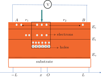
So the peak value of LPV depends on carrier diffusion length λ (or film conductivity σ) significantly. To explain the LPV observed in tin oxide film, we propose the following physical model. Figure 6 shows the schematic profile diagram of the excess carrier diffusion on tin oxide surface under a laser spot illumination. When the film is illuminated by the infrared laser beam (the square light spot area is equal to an area of a circle of about 1 mm in diameter), the electrons will be trapped by the trap level (Et) such as the vacancy energy level. Then some of these electrons will jump into the conduction level, but some still remain in the trap level which can cause additional electrical conductivity. This additional electrical conductivity needs a long time to decay. When the laser illuminates on the film from A to the center of the film then to B, the additional film conductivity σ1 caused by the laser is bigger than σ2 in the case without laser irradiation. Then N(r1) reaching A is bigger than N(r2) reaching B, so the LPV value is produced. As the laser moves from A to O, the more laser irradiations lead to a bigger σ1, thus inducing the peak value of the photovoltage to increase. When the laser spot size reaches –2 mm in diameter on the x axis, the peak value reaches its maximum ∼ 2.24 mV. After that, the competition between σ1 and λz leads to the decrease of the value. when the laser illuminates the center O of the film, that is, r1 equals r2, but the additional σ1 is still bigger than σ2, then N(r1) is bigger than N(r2), so the LPV value is not zero. When the laser spot size reaches 2 mm in diameter on the x axis, the peak value reaches its minimum ∼ 1.78 mV. As the laser moves from O to B, r1 is bigger than r2, but σ1 is still bigger than σ2, so N(r1) is bigger than N(r2) as the additional electrical conductivity is the main factor to the photovoltage. This is why the LPV value is still positive but it decreases. A similar relationship between photovoltaic peak values and the laser positions is obtained when the laser spot moves from B to A, which proves our explanation is reasonable. In fact, λ and σ are autocorrelated and both relate to the film thickness and microstructure of the material including crystal size, orientation, etc. In this polycrystalline film, the study of the dynamic process of carriers flowing under high pressures and temperatures is still progressing. Also, the further measurements of the LPV response of this film under high pressure and temperature are still needed. The preliminary results show that the polycrystalline tin oxide film could be used as an infrared photodetector under 2 MPa pressures.


 , Zhang Ji-Rui5, Shi Hong-Jie5, Yan Kun-Kun5, ‡,