State Key Laboratory for Superlattices and Microstructures, Institute of Semiconductors, Chinese Academy of Sciences, Beijing 100083, China
Synergetic Innovation Center of Quantum Information and Quantum Physics, University of Science and Technology of China, Hefei 230026, China
† Corresponding author. E-mail: zcniu@semi.ac.cn
Project supported by the National Key Basic Research Program of China (Grant Nos. 2014CB643903 and 2013CB932904), the National Special Funds for the Development of Major Research Equipment and Instruments, China (Grant No. 2012YQ140005), the National Natural Science Foundation of China (Grant Nos. 61435012, 61274013, 61306088, and 61290303), and the Strategic Priority Research Program (B) of the Chinese Academy of Sciences (Grant No. XDB01010200).
Abstract
Abstract
We report a type-I GaSb-based laterally coupled distributed-feedback (LC-DFB) laser with shallow-etched gratings operating a continuous wave at room temperature without re-growth process. Second-order Bragg gratings are fabricated alongside the ridge waveguide by interference lithography. Index-coupled LC-DFB laser with a cavity of 1500 μm achieves single longitudinal mode continuous-wave operation at 20 °C with side mode suppression ratio (SMSR) as high as 24 dB. The maximum single mode continuous-wave output power is about 10 mW at room temperature (uncoated facet). A low threshold current density of 230 A/cm2 is achieved with differential quantum efficiency estimated to be 93 mW/A. The laser shows a good wavelength stability against drive current and working temperature.
The semiconductor laser diode based on AlGaAsSb/InGaAsSb alloys grown on GaSb substrates is attracting more and more attention in mid-infrared applications such as remote gas sensing,[1] molecular spectroscopy,[2] medical and defense applications[3] for its small size and excellent laser property. Many industrial and harmful gaseous byproducts such as CO, HF, CO2 and H2O have strong absorption features in the wavelength range between 1.9 μm and 5 μm which is fully covered by GaSb-based laser diode.[4–6] For designing a lidar system for gas sensing, a tunable diode laser absorption spectroscopy (TD-LAS) laser with narrow linewidth is particularly important, which has been reported in previous literature.[1,7,8] GaSb-based Fabry–Perot (FP) laser exhibits mode hops and is inapplicable for this kind of application.[9] Lasers with a mode selecting function such as distributed feedback lasers show excellent characteristics in narrow linewidth and single longitudinal mode emission, thus they are the ideal candidates for gas sensing applications.[10,11]
The conventional fabrication of InP-based DFB lasers emitting around 2 μm requires two to three high-quality epitaxial growths, the first epitaxial process stops after the growth of the waveguide layer, then a Bragg grating structure is fabricated on the wafer, after that, an epitaxial re-growth step is necessary to complete the growth of the laser epitaxy.[12,13] Although the re-growth technique is common and mature in InP-based DFB lasers, it is particularly difficult in the case of GaSb-based laser due to the oxidation of the high Al content in the epitaxy.[14] Miller et al. proposed a regrowth-free DFB structure in which the gratings were located alongside the ridge-waveguide. The laser structure was completed in a single epitaxy layer growth step and avoided the difficulty in the re-growth process. This kind of laser was later named ‘laterally coupled’ DFB (LC-DFB) laser.[15] LC-DFB is aimed at avoiding the oxidation of Al content in the epitaxy after the defining of grating, and it can also be used in GaAs and InP material to avert the re-growth step.[15–17] The GaAs- and InP-based LC-DFB lasers showed a good laser property which was very competitive compared with the traditional DFB laser and attracted a lot of attention.[15–17] So far, the continuous wave operation of GaSb-based LC-DFB laser diodes were reported to emit light beams at wavelengths of 2 μm, 2.3 μm, 2.6 μm, 2.8 μm, 3.4 μm.[5,18–20] Owing to the mode selecting mechanism of LC-DFB lasers, the defining of subsize grating is the most important and difficult part. Among the reports of LC-DFB lasers, Bragg grating has been fabricated using e-beam lithography (EBL),[15,16,21] nanoimprint lithography,[22] and interference lithography.[23] EBL is good at assuring the grating quality but it is expensive and fabrication-inefficient, which is costly and time consuming.[7] Interference lithography and nanoimprint lithography are good at defining Bragg grating on a planar epitaxy surface but they present a big problem in transferring the surface grating deep into the waveguide layer as a high aspect ratio is needed in dry etching. To be specific, the traditional fabrication schedule is first patterning grating on the top of the epitaxy, followed by the defining of the ridge waveguide with photolithography. To form a good coupling coefficient, the ridge waveguide and grating are then etched deep to the waveguide layer in one etching process, which brings problems to the deep dry etching as a high aspect ratio (normally 20:1) is required to transfer the surface grating deep into the waveguide layer.[23]
2. Device design and fabrication
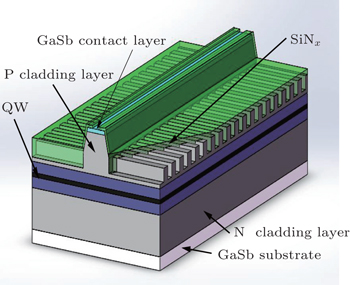
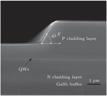
To solve the aforementioned problems and reduce the aspect ratio in dry etching, we report an improved new approach to fabricating an index coupled LC-DFB laser with second-order grating by interference lithography. Figure 1 shows the schematic diagram of our LC-DFB laser structure. This approach enables the fabricating of single-longitudinal-mode lasers following a single epitaxial growth process and the decreasing of the aspect ratio in grating etching. Unlike the traditional defining process of gratings by interference lithography mentioned above,[23] we divide the fabrication of ridge waveguide and grating into two steps; the ridge waveguide is first defined and etched by dry etching and the grating is then formed alongside the ridge waveguide and etched to a shallow depth. The shallow etching of the grating sharply reduces the high aspect ratio in dry etching demanded by the traditional deep etching approach, but shows little loss in the coupling coefficient as it is also etched close to the waveguide compared with the conventional deep etching fabrication, which eventually causes little difference in the laser property. What is more, we have chosen the second-order Bragg grating which further enlarges the etching width and reduces the aspect ratio. As the ridge waveguide is first defined and etched, the epitaxy ready for interference lithography is patterned and has a height difference which will cause problems of photoresist stacking aside the sidewall during interference lithography and eventually make the formation of grating adjacent to the ridge much more difficult. Owing to the coupling principle of LC-DFB, gratings near the ridge are the most important part and have a great influence on laser performance. In order to solve the problem of nonuniform photoresist coating and form a high-quality grating patterned by interference lithography, the ridge waveguide is carefully etched to an inclination of 60° with respect to the horizontal direction, which is an experienced inclination at which the grating quality and laser property reach their equilibrium points after a large number of experiments. Figure 2 shows the scanning electron micrograph (SEM) of the slant ridge waveguide. Owing to the principle of interference lithography, the top of the ridge waveguide is also patterned with a second-order-grating photoresist mask which will be transferred into the ridge waveguide in the grating etching process. The formation of the grating on the ridge waveguide will cause the problem of a contact window opening as a dielectric layer will be deposited after the etching of the grating to form index-coupled mechanism and insulation. The grating on the top of the ridge waveguide is also filled with dielectric. Thus the contact window opening is particularly difficult due to the different selection ratios between dielectric and GaSb material in dry etching which will do harm to the obtainment of p-side Ohm contact and reduce the laser property eventually. To protect the ridge waveguide in the grating etching process and form shallow etching grating adjacent to the ridge waveguide, a SiNx protecting mask needs to be deposited before the defining of the ridge waveguide. During the etching of the grating, the top SiNx layer has a larger section ratio than the AlGaAsSb, thus if the SiNx layer is thick enough, the top GaSb contact layer can be totally protected after the shallow grating etching. To the best of our knowledge this is the first GaSb-based LC-DFB laser with interference-lithography-patterned grating on a non-planar surface. The improved process not only avoids the re-growth of high Al content epitaxy but also reduces the high aspect ratio in grating defining. The laser fabricated by our process emits up to 10-mW light beams in a single longitudinal mode operation at room temperature with an SMSR in excess of 24 dB without facet coating.
Fig. 2. Scanning electron micrograph of the slant ridge waveguide.
The GaSb-based laser structure is grown on an n-type GaSb (100) substrate by using solid–source molecular beam epitaxy (MBE). The epilayer structure contains an n-doped Gasb buffer layer followed by a 1.5-μm n-doped Al0.9Ga0.1As0.02Sb0.98 cladding layer. The undoped active layer consists of 20 nm/10 nm three pairs of In0.2Ga0.8Sb/Al0.4Ga0.6As0.02Sb0.98 quantum wells (QWs) with a compressive strain of 1.0% located in the central part of an undoped 400-nm Al0.4Ga0.6As0.02Sb0.98 waveguide layer.[4] The upper cladding layer is composed of p-doped Al0.9Ga0.1As0.02Sb0.98 layer with a thickness of 1.5 μm followed by a 250-nm highly doped GaSb contact layer for achieving a good Ohm contact with the p-side electrode mental.
The design of our LC-DFB lasers is based on the effective coupling coefficient, the modal effective refractive index of the unperturbed ridge laser is numerically calculated by using a full-vector finite-difference calculation.[21] Assuming an effective-medium index for the grating region, the neff is calculated to be 3.45 while the electric-field overlap factor Γgrating, which describes the extent to which the electric field overlaps with the grating is calculated to be 0.46%, thus the second-order grating width is calculated to be 580 nm for a wave range of 2 μm. Using the approximation employed in Ref. [24], the feedback effect of the lateral gratings can be quantified by estimating the grating coupling coefficient,
where nclad is the index of the upper cladding layer into which the grating is etched, ncover is the index of the SiNx dielectric filling the grating, g is the width of the grating teeth measured to be 240 nm, m is the relevant grating diffraction order, and Λ is the grating pitch. For a cavity length L = 1.5 mm, the κL is estimated to be 1.1, a typical κL value to optimize modal discrimination and optical power.[25]
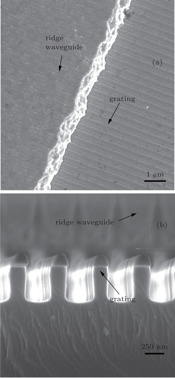
Figure 3 shows a scanning electron micrograph of an LC-DFB laser. A 200-nm SiNx layer is first deposited on the top of the epitaxy using plasma enhanced chemical vapor deposition (PECVD) as etching protecting layer during the shallow etching of gratings. The ridge waveguide is then patterned using contact lithography. The SiNx protecting layer and epitaxy is etched to a total depth of 1.4 μm using an inductively coupled plasma (ICP) with CHF3 and a gas mixture of Ar2 and Cl2 respectively. The sample is then spin-coated with photoresist and the second-order grating is defined alongside the ridge waveguide by interference lithography, due to the thin film of photoresist used in interference lithography, another 100-nm SiNx transferring layer is deposited on the epitaxy before interference lithography to transfer a high quality mask for grating etching. The Bragg grating is first transferred to the SiNx transferring layer by reactive-ion etching (RIE), then the grating is etched to a depth of 400 nm using the SiNx transferring layer as mask by ICP. The ridge waveguide is completely protected in the ICP process as the 200-nm thick SiNx protecting layer on the top of the ridge waveguide remains 100-nm thick after transferring the grating to the SiNx transferring layer, the resulting 100-nm SiNx layer is thick enough to protect the ridge during the grating etching. The shallow etched grating is 150 nm above the active range to form a good coupling with the light. Thus we achieve a high quality grating alongside the ridge waveguide to form a good coupling with the light. Another SiNx layer is deposited on the samples with PECVD after the etching of the grating for insulation and planarization. Finally, an ICP dry etching is used to open a contact window in the SiNx. The p-side top Ohm contacts are formed by Ti/Pt/Au through using a magnetron sputtering system. The bottom Ohm contacts are achieved using fast-annealed alloyed Au/Ge/Ni/Au after wafer thinning of GaSb substrate.
Fig. 3. SEM picture of LC-DFB laser with second-order grating fabricated by interference lithography. (a) Top view of the laser after the deposition of p-side metal (Ti/Pt/Au), (b) sectional view of grating after dry etching.
3. Laser performance
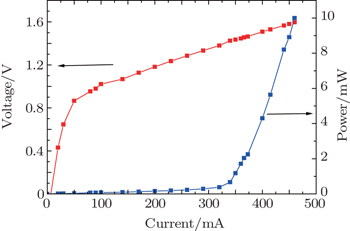
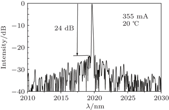
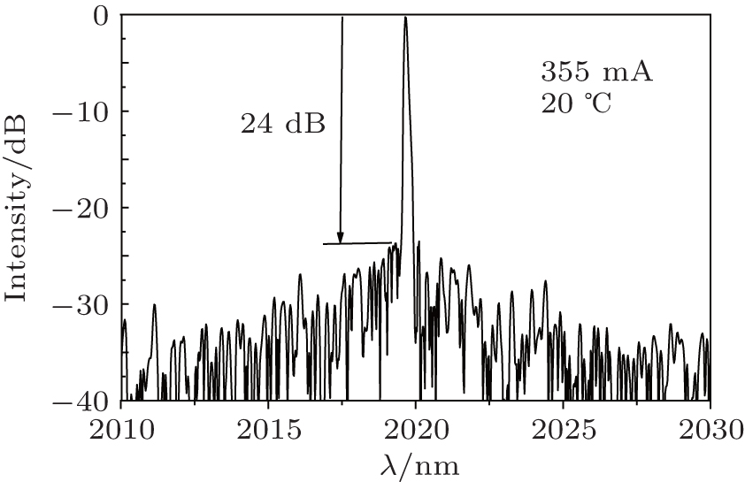
All devices are mounted epi-side down onto a copper heatsink. The output characteristics of these devices are measured using a calibrated thermopile detector at room temperature. Emission spectra are measured by a Fourier-transform infrared (FTIR) method. All the devices are tested without facet coating. Figure 4 shows the power–current–voltage (P–I–V) characteristics of the laser at room temperature in continuous wave (CW) regime. The laser shows a low threshold current density of Jth = 230 A/cm2 with a ridge waveguide length of 1500 μm. Thus the differential quantum efficiency is estimated to be 93 mW/A. With a bias current of 440 mA, the LC-DFB emits up to 10 mW from both facets at 20 °C. At high drive current, the gain spectrum is red-shifted and the output power is limited by thermal roll-over. A turn-on voltage of 0.8 V shows Ohm contact between the epitaxy and the metal. However, the operation voltage increases quickly with increasing drive current which is mainly caused by the large series resistance. This can be improved by optimizing the Ohm contact between the metal and epitaxy. Figure 5 shows a representative output spectrum of our LC-DFB. At a drive current of 355 mA the laser shows a single longitudinal mode operation with a side-mode suppression ratio (SMSR) as high as 24 dB.
Fig. 5. Representative output spectrum of an LC-DFB laser with an injecting current of 355 mA. The laser shows a single longitudinal mode operation with an SMSR of 24 dB.
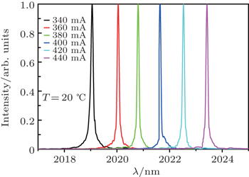
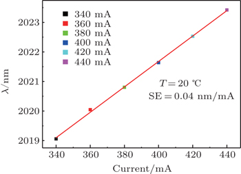
The light against current (L–I) characteristics at room temperature are shown in Figs. 6 and 7. The uncoated LC-DFB laser is operated in a single longitudinal mode near 2 μm. The wavelength shifted towards longer wave range linearly with the increasing of injecting current. When the drive current increases from 340 mA to 440 mA, the emission wavelength shifts from 2019.05 nm to 2023.42 nm. The slope is estimated to be about 0.04 nm/mA. When the drive current is above 450 mA, multimode emission is observed due to the aggravated thermal effect, which causes the mismatch between gain spectrum and the grating wavelength.
Fig. 7. Wavelength shifts of LC-DFB laser at different injection currents at 20 °C.
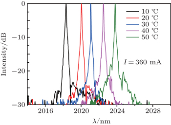
The light against temperature characteristics are shown in Fig. 8. Under a drive current of 360 mA, the output spectrum shows the emission wavelengths at different heatsink temperatures. The wavelength shifts from 2018.34 nm to 2023.82 nm in a temperature range from 10 °C to 50 °C. The slope is estimated to be 0.14 nm/°C. This slope is most likely determined by the change in effective index of the laser structure. Our LC-DFB shows a good temperature stability as the slope is about one tenth of that in the case of Fabry–Perot laser, whose wavelength shifts more freely with the drifting of the gain peak in the gain spectrum. At a high working temperature, we can also observe a decrease in SMSR.
Fig. 8. Spectral intensities against wavelength for different working temperatures at a drive current of 360 mA.
4. Conclusions
We successfully present an improved fabrication of LC-DFB laser which is low cost and productive. The second-order etched grating is patterned by interference lithography on a nonplanar epitaxy. Our improved fabrication sharply reduces the aspect ratio of the conventional process without loss of laser property. The epitaxy is completed in a single growth step and avoids the regrowth of oxidated Al content in epitaxy layer. The CW laser operates in a single longitudinal mode at room temperature with an SMSR of more than 24 dB. The wavelength stability against current and temperature shows a typical characteristic of laterally coupled distributed feedback laser. The device emits up to 10 mW at room temperature which is high enough for gas sensing application in mid-infrared wavelength.


 ]
]