†Corresponding author. E-mail: wangguangqiang@nint.ac.cn
*Project supported by the National Natural Science Foundation of China (Grant No. 61231003).
By investigating the interaction of an n-type silicon sample with the TM01 mode millimeter wave in a circular waveguide, a viable high-power TM01 millimeter wave sensor is proposed. Based on the hot electron effect, the silicon sample serving as a sensing element (SE) and appropriately mounted on the inner wall of the circular waveguide is devoted to the on-line measurement of a high-power millimeter wave pulse. A three-dimensional parallel finite-difference time-domain method is applied to simulate the wave propagation within the measuring structure. The transverse electric field distribution, the dependences of the frequency response of the voltage standing-wave ratio (VSWR) in the circular waveguide, and the average electric field amplitude within the SE on the electrophysical parameters of the SE are calculated and analyzed in the frequency range of 300–400 GHz. As a result, the optimal dimensions and specific resistance of the SE are obtained, which provide a VSWR of no more than 2.0, a relative sensitivity around 0.0046 kW−1 fluctuating within ± 17.3%, and a maximum enduring power of about 4.3 MW.
There have been extensive demands on the compact highpower millimeter wave sources due to their unique physical properties for numerous applications, including in radars, communications, plasma heating, and in a directed-energy weapon.[1, 2] So far, gyrotrons[3– 5] and relativistic Cerenkov oscillators[6– 10] have shown the merits of compactness and high-power up to the MW level. Circular waveguides are widely used in these two types of sources to generate and propagate high-power millimeter wave pulses of TE or TM mode. Generally, coupling structures, including aperture and probe in the circular waveguide, are adopted to achieve the on-line measurement of the high-power pulse. There are two objectives to use such an on-line measurement. One is for the sake of comparison of the measured results with those obtained by using another method, such as the far-field measurement, [8] and hence it is used as a supplement method. The second is to monitor the waveform of the generated wave in the time domain, and the rise time and duration of the generated pulse are obtained. However, the dimensions of the coupling structures rapidly scale down with the increase of frequency, [11] making their manufacture difficult and expensive at the millimeter wave bands. Kancleris et al. studied a resistive sensor for measuring the high-power microwave (HPM) pulse of the TE01 mode in a circular waveguide, [12, 13] and theoretically estimated its maximum enduring power of 2.2 MW in the X band. Although the power level is too low for the on-line measurement of the HPM pulse, this edifies us to attempt the online measurement of the high-power millimeter wave pulse using the hot electron effect of silicon under a high electric field. Until now, there have been no public reports concerning the research of other usual modes or at higher frequency bands in a circular waveguide.
In this paper, we propose a sensing structure based on the hot electron effect of n-type silicon for the measurement of the high-power millimeter wave pulses of the TM01 mode in a circular waveguide. Using a three-dimensional parallel finite-difference time-domain (FDTD) method, the interaction between the silicon sensing sample and the millimeter wave of the TM01 mode is numerically investigated. Combined with theoretical estimations, the more appropriate electrophysical parameters of the sensing structure and some key performances are determined so that it could serve as an alternative device for the on-line measurement of the kW-class millimeter wave pulse of the TM01 mode in the frequency range of 300– 400 GHz.
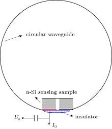
Referring to our previous work on the resistive sensors (RS) used in a rectangular waveguide, [14– 16] the sensing structure for the millimeter wave of the TM01 mode in a circular waveguide is proposed and shown in Fig. 1. The sensing element (SE) is designed to be a plate consisting of two separate n-Si blocks placed in close proximity to each other. The upper contacts of the two silicon blocks are shorted with a thin copper foil, and the bottom contact of one silicon block is grounded with the waveguide wall while the other is isolated from the waveguide and connected to a connector of SMA type, serving as the bias current feed and the output signal measurement. The interspace beneath the SE is occupied by an appropriate isolating material to avoid the stress-induced distortion and breakage of the SE. This configuration is convenient for assembly, and the SE only “ feels” the electric field component Er, as long as the dimensions of the SE are small enough compared with the radius of the circular waveguide, because other components of the regular TM01 wave are zero in the vicinity of the waveguide wall.
Let us consider the sensitivity of the proposed sensing structure for TM01 mode millimeter wave with power Pin in the circular waveguide. According to the scattering theory of electrons in a semiconductor, the resistance change Δ R/R0 of the SE under a high electric field satisfies the equation[14]

where β * is the effective warm electron coefficient, [17] and 〈 E〉 is the average electric field amplitude in the SE. With constant bias current I0, the relative sensitivity is defined as

where Us and U0 are the output and the bias voltages, respectively.
Using the expression defining the power flow of TM01 mode in a circular waveguide, one can obtain the sensitivity over a wider range of power levels as follows:

where f and fc are the frequency of the measured millimeter wave and the cut-off frequency for the TM01 mode, respectively; J1 is the first kind Bessel function of the first order; x01 = 2.405 is the first root of J0; R is the radius of the circular waveguide; and, Emax denotes the maximum amplitude of the electric field component Er of the regular TM01 wave in the empty waveguide. When the measured pulse power is not so high that Δ R/R0 ≪ 1, then expression (3) goes over to

with Eq. (1). This is the sensitivity in the linear region. Obviously, there is only one unknown parameter, i.e., 〈 E〉 , in Eqs. (3) and (4) for a certain sensing structure. Thus, calculating it is critical for the optimal design of the sensing structure.
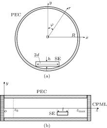
As one of the most popular computational electromagnetics algorithms, the three-dimensional (3D) finite-difference time-domain method[18] is applied to compute the electric field distributions in the proposed sensing structure. The modeled section of the circular waveguide with SE is shown in Fig. 2. The SE is treated as a whole rectangular obstacle with a perfect conductor layer on the top, ignoring the interspace between the two n-Si blocks. Beneath the SE, the isolating filler is air. The wall of the circular waveguide is regarded as a PEC boundary that has several layers.
To deal with the numerical singularity of the FDTD scheme in cylindrical coordinates at r = 0, [18] we use the Cartesian coordinate system to calculate all of the components of the electromagnetic field, and then transform them all to ones in cylindrical coordinates. This method is also convenient and exact to mesh and solve the model of the SE. In the plane z = z0, the TM01 type sinusoidal wave is excited, and the CPML[19] is mathematically specified in the planes z = 0 and z = zmax. The obstacle of the SE is placed at about one wavelength ahead the excitation plane and at a shorter distance before the end of the modeled waveguide.
Circular waveguides with large diameters are often used to generate and propagate the intense millimeter wave pulses in relativistic Cerenkov oscillators.[6– 10, 20, 21] To avoid the excitation of other modes to the greatest extent, the thickness of the SE should be as small as possible to have little influence on the electric field distributions and sufficiently “ feel” the Er of the TM01 mode wave. Thus, the 3D FDTD program is paralleled based on the MPI platform to obtain a fine mesh of the SE and accurate simulation results. Hence, the calculation time is reduced greatly.
All of the simulations are performed for a circular waveguide with radius of R = 4.5 mm, which was used as an output waveguide in a 0.34 THz high-power surface wave oscillator.[21] The dimensions and the specific resistance of the SE are verified to investigate the electric field distribution and the dependences of voltage standing wave ratio (VSWR) and electric field strength in SE on frequency, seeking out the appropriate structural parameters of the proposed sensing structure. The maximum electric field amplitude of the regular TM01 wave in the empty waveguide is set to be unit.
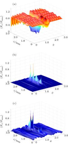
Distributions of electric field components Er, Eφ , and Ez at the frequency of 340 GHz in the φ 0z plane that lies at the midpoint of the height of the SE are shown in Fig. 3. In this example, the SE has the specific resistance ρ = 2 Ω · cm and dimensions h × 2d × l = 0.3 mm × 1.2 mm × 1.0 mm. As one can see from the figure, the SE distorts the regular electric field distributions of the TM01 wave. The regular perturbation of component Er is found along z and φ directions, and becomes significant just before the SE. Distinguished from those in the empty waveguide, components Eφ and Ez are excited in the neighborhood of the SE with very large amplitudes and are concentrated on its outer surfaces. This is caused by the abrupt change of medium permittivity between air and silicon, and is also observed in the rectangular resistive sensor.[15, 16] Nevertheless, each electric field component out of the SE accords well with the theoretical ones of the TM01 wave in the empty waveguide, implying that no other modes are excited in the circular waveguide due to the insertion of the SE. Meanwhile, the average electric field in the SE mostly consists of the Er component, while the average value of Ez is roughly 10 times less and that of Eφ is more than 20 times less. This confirms that the SE in our proposed sensing structure indeed only “ feels” the electric field in one direction.
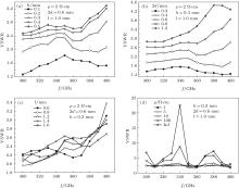
The perturbation of component Er can be described by VSWR, indicating the reflections in the sensing structure caused by the SE. Dependences of VSWR on frequency for different dimensions and specific resistances of the SE are calculated and shown in Fig. 4. In the 300– 400 GHz frequency range, VSWR increases monotonously and obviously with the height and the width, which determines the area of the cross section of the SE. The relative variation of VSWR versus length of the SE is not apparent, whereas its variation range is basically not changed for the fixed cross section. The specific resistance affects VSWR to some extent, and increasing ρ leads to its sharp growth at certain frequencies, such as 300 GHz, 340 GHz, and 380 GHz. Therefore, reducing the area of the cross section and choosing a smaller specific resistance help to get VSWR as small as possible in the proposed sensing structure.
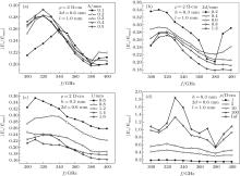
The average electric field strength in the SE determines the relative sensitivity of the sensing structure, and has a great influence on the flatness of the frequency response according to Eq. (4). Dependences of 〈 E/Emax〉 on frequency for different dimensions and specific resistances of the SE are presented in Fig. 5. Our calculation results reveal that 〈 E/Emax〉 in the SE increases first at low frequencies, but it then decreases until the frequency approaches 380 GHz or higher. The height has no remarkable effect on the average electric field strength while the other three parameters have. The SE with smaller width and length, and larger specific resistance can provide a more sensitive sensing structure for the TM01 mode in the circular waveguide. However, all of the four parameters affect the variation range of the frequency response of 〈 E/Emax〉 , and consequently the relative sensitivity variation. To obtain a flat frequency response, there should be a slight decrease of the average electric field with frequency to compensate for the tiny sensitivity increase caused by the wave dispersion in the circular waveguide. As seen from Fig. 5, keeping the height and specific resistance of the SE as small as possible and selecting moderate width and length seem to be a good choice.
To be a sensing structure with excellent performance, our proposed sensing structure should meet the following main requirements. First, the reflection in the waveguide induced by the SE should be as small as possible, as is the value of VSWR. Second, the initial resistance of the SE should be in the vicinity of 50 Ω to match the external circuits and have a response time in the picosecond level.[14] Finally, a flat frequency response of relative sensitivity in the 300– 400 GHz range is preferable. Besides, it is worth mentioning that the ranges and precisions of parameters that can reach for practical n-Si materials used for the SE should be considered before proceeding with finetuning of the parameters to optimize the sensing structure.
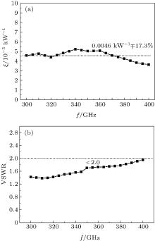
Based on the response characteristics of the SE to the TM01 wave in the circular waveguide, the following electrophysical parameters of the SE are selected after dozens of numerical simulations: ρ = 2 Ω · cm, h × 2d × l = 0.2 mm× 0.4 mm × 0.8 mm. Its initial resistance is just 50 Ω . The present dependences of the relative sensitivity in the linear region and VSWR on frequency are shown in Fig. 6. The calculated sensitivity of the optimal sensing structure within the 300– 400 GHz range is roughly 0.0046 kW− 1 with a variation of ± 17.3%, and the calculated VSWR is controlled to be less than 2.0. These are the best results so far found for the proposed sensing structure.
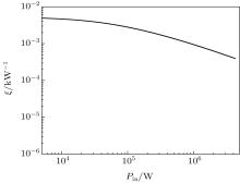
As an important performance parameter, the maximum enduring power of the proposed sensing structure is estimated theoretically. On the one hand, due to the hot-electron effect, the allowed maximum electric field strength applied on n-Si is about 20 kV/cm, [17] and the electric field strength in the SE is probably a quarter of Emax for our optimal sensing structure. On the other hand, the electric field strength limit of bigger than 100 kV/cm in the circular waveguide due to RF breakdown is considered, [22] since the sensing structure directly connected to the measured millimeter wave source for on-online measurement has a near-vacuum. Thus, the maximum value of Emax is about 80 kV/cm, and accordingly the maximum transmitted power in the proposed sensing structure is calculated to be 4.3 MW. From this value we can infer that our proposed sensing structure could be directly used for the on-line measurements of millimeter wave sources with a power level as high as several megawatts. The dependence of the relative sensitivity on power up to the maximum enduring power is estimated with the help of Eq. (3) and is shown in Fig. 7. Roughly 90% decrease of ξ is found at the maximum power due to the nonlinear effects. Fortunately, the decrease of the absolute sensitivity can be compensated to some extent by increasing the bias current.
A sensing structure for high-power TM01 wave in the circular waveguide is proposed, and the response of an n-Si sample within it to the TM01 wave in the 300– 400 GHz range is numerically investigated. It is found that the SE only “ feels” the electric field component Er while the other two components are negligible in the proposed structure. By adjusting the electrophysical parameters of the SE, we obtain the optimal sensing structure with small VSWR and sensitivity variation at a moment. For the TM01 wave within the 300– 400 GHz range, the calculated sensitivity is about 0.0046 kW− 1 with a variation of 17.3%, and VSWR is less than 2.0, which implies a power reflectance of 11%. The maximum enduring power as high as 4.3 MW further confirms that it could serve as an alternative device for the on-line measurement of TM01 wave up to the MW class. The proposed sensing structure here is being fabricated and is going to be tested in the 0.34 THz high-power surface wave oscillator (SWO). The particle simulation and preliminary experiment show that this high power SWO can generate a signal with a frequency of 320– 350 GHz, a duration of 2 ns, and a radiation power of more than 250 kW.[20, 21]
| 1 |
|
| 2 |
|
| 3 |
|
| 4 |
|
| 5 |
|
| 6 |
|
| 7 |
|
| 8 |
|
| 9 |
|
| 10 |
|
| 11 |
|
| 12 |
|
| 13 |
|
| 14 |
|
| 15 |
|
| 16 |
|
| 17 |
|
| 18 |
|
| 19 |
|
| 20 |
|
| 21 |
|
| 22 |
|


