


Realizing mode conversion and optical diode effect by coupling photonic crystal waveguides with cavity
[Ye Han†,‡a)  , Zhang Jin-Qian-Nan
a) ‡ , Yu Zhong-Yuana) , Wang Dong-Linb) , Chen Zhi-Huic) ]
, Zhang Jin-Qian-Nan|
|


†Corresponding author. E-mail: Han_ye@bupt.edu.cn
‡These authors contributed equally.
*Project supported by the National Natural Science Foundation of China (Grant Nos. 61372037 and 61307069), Beijing Excellent Ph. D. Thesis Guidance Foundation, China (Grant No. 20131001301), and the Natural Science Foundation of Shanxi Province, China (Grant No. 2013021017-3).
We propose a novel two-dimensional photonic crystal structure consisting of two line defect waveguides and a cavity to realize mode conversion based on the coupling effect. The W1/cavity/W2 structure breaks the spatial symmetry and successfully converts the even (odd) mode to the odd (even) mode in the W2 waveguide during the forward (backward) transmission. When considering the incidence of only the even mode, the optical diode effect emerges and achieves approximate 35 dB unidirectionality at the resonant frequency. Moreover, owing to the narrow bandpass feature and the flexibility of the tuning cavity, utilization of the proposed structure as a wavelength filter is demonstrated in a device with a Y-branch splitter. Here, we provide a heuristic design for a mode converter, optical diode, and wavelength filter derived from the coupling effect between a cavity and adjacent waveguides, and expect that the proposed structure can be applied as a building block in future all-optical integrated circuits.
Owing to the capability of the unidirectional propagation of an electrical current, the semiconductor diode has acted as a fundamental component of transistors, logic gates, and integrated circuits, which led to the evolution of information technology in the last decades. The counterpart structure for asymmetric light propagation, which is referred to as the optical diode, has attracted considerable attention due to its potential applications in next-generation all-optical computing and information processing.[1– 6] The magneto-optical effect[7– 12] and optical nonlinearity[13– 17] are conventionally utilized to break the reciprocity and obtain the unidirectional transmission. Unfortunately, common optoelectronic materials, including most semiconductors, present only relatively weak or even no magneto-optical effect. Meanwhile, the high operational intensity threshold of the nonlinear effect also limits its usage Therefore, linear and passive structures with an optical diode effect are highly desirable. One promising candidate is the photonic crystal (PhC) which has broken spatial symmetry while still keeping the reciprocity.[18– 25]
The unidirectional transmission in a linear and passive PhC structure can be realized by a mode conversion in a spatial asymmetric manner. Several schemes have been proposed. Wang et al.[18, 19] designed a wavelength-scale PhC heterojunction, which comprised two silicon square lattice PhC slabs with air holes of different radii. The heterojunction introduced a directional bandgap mismatch and different mode transitions along the Γ M direction.[18– 21] By breaking the spatial inversion symmetry, the mode conversion led to an optical diode effect and the forward transmission efficiency reached 20% at peak in the experiment after optimization. Liu et al.[22] presented a compact mode converter using a two-step numerical optimization process and applied it to the optical diode. This approach used the combinatorial search on an area of 5× 4 rods in the line defect waveguide to obtain a set of candidates that performs high efficient even– odd mode conversion. A further optimization adjusted the radii of the existing rods in the area. Feng et al.[23] proposed a unidirectional reciprocal wavelength filter based on the coupling between a rectangular defect and two perpendicular PhC waveguides. The output waveguide was specially designed to accommodate both even and odd modes. The wavelength was selected by designing the spatial coupling position based on the mode profile of the rectangular defect at the corresponding resonant frequency. The forwarding transmission was about 25% in a two-dimensional simulation. More recently, Khavasi et al.[24] reported a pure PhC waveguide optical diode. The waveguide had two paths: the fields propagating through the two paths had a phase difference, and they then converged to realize the even– odd mode conversion. To ensure the unidirectionality, a specific mode filter was needed to block the even mode in the backward direction.
In this paper, we design a new PhC based optical diode with high transmission efficiency, high unidirectionality, and high-level symmetry of input/output ports. The proposed W1/cavity/W2 structure breaks the spatial symmetry and successfully realizes the even– odd mode conversion in the W2 waveguide. The electric field and the transmission efficiency are numerically simulated by using the two-dimensional finite element method (FEM). Due to the intrinsic profile match and the mismatch between the waveguide mode and the cavity mode, the structure shows high unidirectionality for the even mode.
The design is based on a two-dimensional square lattice PhC made of silicon rods immersed in air. The lattice constant is a and the radius of the rod is 0.2a, which is commonly used in the previous studies.[22– 24] The relative permittivity of silicon is ε = 12 in the near-infrared wavelength range. As depicted in Fig. 1, the proposed PhC structure simply consists of two line defect waveguides and a cavity. We define the left to right as the forward direction and the opposite as the backward direction. Along the forward route, the PhC structure can be divided into five parts: 1) W2 waveguide made by removing two rows of rods; 2) a four-column length matching stage; 3) W1 waveguide made by removing one row of rods; 4) L2 cavity with two central rods removed; and, 5) W2 waveguide. By vertically shifting the neighbor three rows of rods by − 0.2a per column, the tapered matching stage which connects W2 and W1 waveguides is constructed to avoid the back reflection induced by sudden waveguide narrowing. The sandwich-like W1/cavity/W2 coupling structure breaks the spatial symmetry, which is used to achieve the mode conversion and unidirectional optical transmission. Considering it as a black box in photonic systems/circuits, we intentionally arrange the input and output ports with a high-level of symmetry by introducing the W2 waveguide and the matching stage, which would benefit the integrated features.
For the square lattice PhC formed by silicon rods with 0.2a radius, the first photonic band gap for TM-polarized modes (electric vector parallel to rod) is from frequency 0.281c/a to 0.417c/a, where c is the light speed in vacuum. The W2 waveguide based on the above PhC can support both even and odd modes, between which the mode conversion is pursued in this paper. Figure 2(a) demonstrates the dispersion curve for each mode calculated by scanning the wave vector at the Γ X direction in FEM. As an example, the electric fields of odd mode and even mode at frequency 0.3750c/a are shown. It should be noted that the lowest frequency of the odd mode is 0.3526c/a at the Γ point, indicating that the mode conversion is only available for higher frequencies. Moreover, the L2 cavity is another key component. Besides removing two central rods, we vertically shift two neighboring rods (up and down, respectively) by Λ = 0.2a, as shown in Fig. 2(b). The eigenfrequency analysis in FEM is used to determine the cavity modes. The first mode at 0.3292c/a possesses even spatial symmetry in both horizontal and vertical directions, while the second mode at 0.3930c/a is even symmetric in the horizontal direction and odd symmetric in the vertical direction. The similarity between the second cavity mode and the odd mode in the W2 waveguide is the cornerstone for the mode conversion.
 | Fig. 1. Schematic diagram of the proposed two-dimensional PhC mode converter and optical diode. The structure can be divided into five parts (from left to right): W2 waveguide, matching stage, W1 waveguide, L2 cavity, and W2 waveguide. PhC is based on silicon rods (ε = 12) in air. |
 | Fig. 2. (a) Dispersion curves of even mode and odd mode supported by the W2 waveguide. The inset shows mode profiles at frequency 0.3750c/a. (b) Schematic diagram and two mode profiles of the L2 cavity with Λ = 0.2a. |
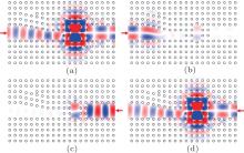
To explicitly interpret how the proposed PhC structure works as a mode converter or an optical diode, four scenarios are considered hereinafter: even/odd mode incident from port 1/2. Figures 3(a)– 3(d) illustrate the electric field profiles simulated by FEM for scenarios I– IV with input light at frequency 0.3930c/a, which is identical to the resonant frequency of the second L2 cavity mode. The light propagating direction is indicated by the red arrow.
 | Fig. 3. Electric field profiles with input light at frequency 0.3930c/a: (a) even mode and (b) odd mode excited at port 1; (c) even mode and (d) odd mode excited at port 2. The red arrow indicates the light propagation direction. |
For scenario I, the even mode is excited at port 1 as depicted in Fig. 3(a). The even mode in the W2 waveguide propagates forward, through the matching stage in which the mode is spatially compressed, and then enters the W1 waveguide. Due to the frequency and mode profile match, the even mode in the W1 waveguide couples to and stimulates the second L2 cavity mode. Finally, the cavity mode couples to the odd mode in the W2 waveguide on the right side based on the same principle. Consequently, the conversion of the even mode to the odd mode is realized with a transmission efficiency about 92.5%. For scenario II, the odd mode is excited at port 1, as shown in Fig. 3(b). The odd mode propagating forward is obviously obstructed by the matching stage, which nicely behaves as a mode filter, because the gradually narrowed waveguide does not support the odd mode. Since little power is transmitted to couple with the L2 cavity, port 2 will scarcely have any outgoing light. For scenario III, the even mode is excited at port 2, as depicted in Fig. 3(c). Because of the mismatched mode profile, the L2 cavity mode is not stimulated and it successfully blocks the even mode in the W2 waveguide. For scenario IV, the odd mode is excited at port 2, as shown in Fig. 3(d). The odd mode propagates backward and reaches the right side of the cavity. As demonstrated earlier, the odd mode has a similar profile with the second L2 cavity mode and thus coupling occurs. The stimulated cavity mode then couples to the even mode in the W1 waveguide and exits port 1, also keeping the even symmetry in the W2 waveguide. The conversion of the odd mode to the even mode, which is opposite to scenario I, is achieved in backward transmission.
The similarity between the electric field profiles in Figs. 3(a) and 3(d) clearly shows the reciprocity of the linear W1/cavity/W2 coupling structure with broken spatial symmetry, which leads to mutual even– odd mode conversion in forward and backward transmissions. More importantly, in scenarios I and III, the proposed PhC structure is proven to possess the optical diode effect. The corresponding transmission spectra for the incidence of even mode, denoted as solid (forward) and dashed (backward) lines, are plotted in Fig. 4. Due to the L2 cavity involved coupling, light within a narrow frequency range can pass forward through the PhC structure. The full width at half maximum is about 0.0002c/a. The forward transmission efficiency reaches a maximum at frequency 0.3930c/a, while the efficiency stays below 0.1% within the frequency range from 0.3900c/a to 0.3960c/a for the backward transmission. Approximate 35 dB unidirectionality is achieved at the resonant frequency, which is at the same level as a recent PhC optical diode design.[19] Moreover, it should be noted that the simulation is performed for a two-dimensional model which has not included the radiation loss (parallel to rods) in real three-dimensional PhC devices.
 | Fig. 4. Forward and backward transmission spectra of the proposed PhC structure with incidence of even mode. The inset shows the electric field profiles with input light at frequency 0.3930c/a. |
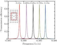
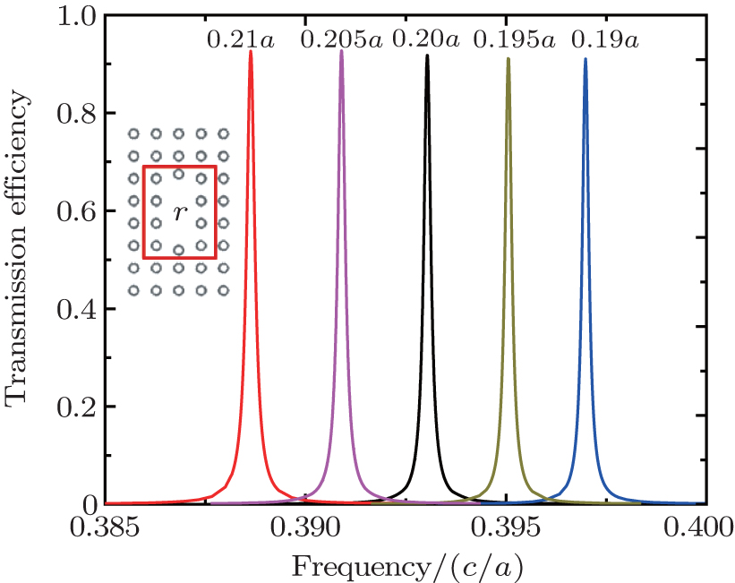
As discussed previously, the proposed PhC structure inherently possesses a low bandpass feature due to the cavity involved coupling. The peak of the transmission spectrum is determined by the resonant frequency of the second L2 cavity mode, which can be tuned by altering attributes and the spatial distribution of rods in the cavity region. Accordingly, huge design flexibility is provided while keeping the desired cavity mode profile is essential. Figure 5 demonstrates the forwarding transmission spectra when modifying the radius of 10 rods in the red box. These rods are the nearest rods surrounding the defect of the L2 cavity. The presented radius range is from 0.19a to 0.21a with step 0.005a. The corresponding peaks of the spectra can be fitted by f = 0.3889 + 0.464(r/a) − 2.2167(r/a)2 (0.18a < r < 0.22a). Moreover, the forwarding transmission spectra of modifying movement Λ of two specific rods in the L2 cavity are illustrated in Fig. 6. The presented movement range is from 0.15a to 0.25a with step 0.025a. The corresponding peak frequencies can be fitted by f = 0.4112 − 0.0999(Λ /a) + 0.0459(Λ /a)2 (0.1a < Λ < 0.3a). All of the structures achieve commendable unidirectionality because the maximum forward transmission efficiencies exceed 90%.
 | Fig. 5. Forward transmission spectra of the proposed PhC structures with modified radii of the specific rods in the L2 cavity region, where r denotes the radius of the rods inside the red box. |
 | Fig. 6. Forward transmission spectra of the proposed PhC structures with modified movements of two specific rods in the L2 cavity, where Λ denotes the movement of two rods beside the red arrows. |
Three key features (unidirectional transmission, narrow bandpass, and flexibility on tuning the center frequency) make the proposed PhC structure a combination of optical diode and wavelength filter. As an example, we construct a Y-branch splitter with the coupling structure on each arm. The radii of rods in the red box (Fig. 7(a)) are different: r1 = 0.19a for the upper arm and r2 = 0.2a for the lower arm. For the forward transmission, the incident light (even mode) propagates from port 1 and then splits into two beams. When the light frequency is close to one of the L2 cavities’ resonant frequencies, the corresponding output port (port 2 or port 3) will export light (odd mode) due to the mode conversion achieved by coupling between the cavity and adjacent waveguides, as demonstrated in Figs. 7(c) and 7(d). Otherwise, the cavity will block the forward light in the W1 waveguide. For the backward transmission, as shown in Fig. 7(b), even modes at frequencies 0.3970c/a and 0.3930c/a are excited at port 2 and port 3, respectively. The lights are blocked due to the mode profile mismatch between the even mode in the W2 waveguide and the second L2 cavity mode.
 | Fig. 7. (a) Schematic diagram of Y-branch wavelength filter with optical diode effect. (b) Simulated electric field profile of even modes at frequencies 0.3970c/a and 0.3930c/a incident from port 2 and port 3, respectively. (c) and (d) Simulated electric field profiles of even mode at frequencies 0.3970c/a and 0.3930c/a incident from port 1. |
A two-dimensional square lattice PhC structure comprising two line defect waveguides and a cavity is designed to realize mode conversion based on a simple coupling effect. The spatial asymmetric W1/cavity/W2 structure successfully converts even mode to odd mode in the W2 waveguide during the forward transmission, and vice versa. For the incidence of the only even mode, the optical diode effect emerges and achieves high unidirectionality. The forward transmission efficiency keeps above 90% and unidirectionality reaches approximate 35 dB. The flexibility of tuning the resonant frequency of the L2 cavity is demonstrated by adjusting the radii and the movement of the rods. Moreover, based on the narrow bandpass feature, we construct a Y-branch splitter in which the proposed structure works as a wavelength filter. Here, we provide a heuristic design based on coupling between cavities and adjacent waveguides for mode converter, optical diode, and wavelength filter, and expect that the results will help develop the recipes for future PhC devices in all-optical integrated circuits.
| 1 |
|
| 2 |
|
| 3 |
|
| 4 |
|
| 5 |
|
| 6 |
|
| 7 |
|
| 8 |
|
| 9 |
|
| 10 |
|
| 11 |
|
| 12 |
|
| 13 |
|
| 14 |
|
| 15 |
|
| 16 |
|
| 17 |
|
| 18 |
|
| 19 |
|
| 20 |
|
| 21 |
|
| 22 |
|
| 23 |
|
| 24 |
|
| 25 |
|