


Electronic structure of silicene
[L. C. Lew Yan Voon† ]
]
]
|
|


†Corresponding author. E-mail: llewyanv@citadel.edu
*Project supported by the Citadel Foundation.
In this topical review, we discuss the electronic structure of free-standing silicene by comparing results obtained using different theoretical methods. Silicene is a single atomic layer of silicon similar to graphene. The interest in silicene is the same as for graphene, in being two-dimensional and possessing a Dirac cone. One advantage of silicene is due to its compatibility with current silicon electronics. Both empirical and first-principles techniques have been used to study the electronic properties of silicene. We will provide a brief overview of the parameter space for first-principles calculations. However, since the theory is standard, no extensive discussion will be included. Instead, we will emphasize what empirical methods can provide to such investigations and the current state of these theories. Finally, we will review the properties computed using both types of theories for free-standing silicene, with emphasis on areas where we have contributed. Comparisons to graphene is provided throughout.
The term silicene was introduced by Guzmá n-Verri and Lew Yan Voon[1] to denote a single atomic layer of silicon (Si) with the structure of graphene.[2] It turns out that there were earlier works, both theoretical[3– 7] and experimental.[8, 9] They went mostly unnoticed until silicene nanoribbons were reported to have been fabricated on a silver substrate in 2009.[10] The most reliable reports of silicene itself, grown on Ag (111), started in 2012.[11– 15] The growth was achieved under ultrahigh vacuum conditions by evaporation of a piece of silicon wafer and the slow deposition of Si atoms onto the Ag substrate at 220 ° C– 260 ° C.
To date, no free-standing silicene has been reported. Nevertheless, it is important to understand its properties before investigating how the properties might be altered by the presence of a substrate, by functionalization or in a device structure. Indeed, a field-effect transistor made out of silicene has finally been demonstrated in 2015.[16]
In this article, we focus on topics we have contributed towards. Additional topics are treated based upon their importance.
Four primary methods have been used to date to study the structure and electronic properties of silicene.
Predicting the structure has been the mainstay of quantum- mechanical first-principles methods. They are invariably based upon density functional theory (DFT), whether using the local-density approximation (LDA) or the generalized-gradient approximation (GGA) to the exchange– correlation potential.[17] This is an approximate solution to the many-body Schrö dinger equation. The LDA is known to lead to overbinding and, therefore, a slightly smaller lattice constant. In principle, it is only necessary to be given the atomic number of the atoms present and the theory predicts the most stable stucture. However, computational constraints dictate maintaining a given lattice symmetry. The procedure is to assume an initial geometry and then the atoms are moved so as to minimize the total energy while preserving the lattice symmetry. Once the structure is obtained, one can compute the corresponding electronic structure and electronic properties. For silicene, the crystal structure consists of two atoms per unit cell and the structure is two-dimensional (2D). Since the stadard DFT codes assume periodicity in three dimensions, a supercell technique is used to generate an artificial periodicity in the third dimension; at least 15 Å is needed to electronically decouple the layers. As an example, Sandberg et al.[18] used the ABINIT DFT package[19, 20] with Troullier– Martin pseudopotentials and a plane wave basis set. Convergence tests showed that a 40-Hartree cutoff was sufficient for all of the calculations (1 Hartree= 27.2114 eV). They optimized the geometry of the systems using the Broyden– Fletcher– Goldfarb– Shanno minimization scheme, and a 10− 4-Hartree/Bohr tolerance on the maximal force on the atoms. They allowed smearing of the energy cutoff by 0.5 Hartree, and a maximal scaling of the lattice dimensions of 1.1. The supercell' s shape, volume, and ionic positions were all given the freedom to relax. They used a 10− 8-Hartree tolerance on the difference of total energy which when reached twice in succession ended a self-consistent field (SCF) cycle. They used a macroscopic dielectric constant of 12 (which is standard for semiconductors) to speed the convergence of the SCF cycles. The k-point grid was generated using a 2× 2 × 2 Monkhorst– Pack grid, based on the primitive vectors of the cell, which ABINIT then shifted four times.
An alternative method that has been used mainly for studying the mechanical properties has been classical molecular dynamics (MD) of a large system of many atoms, usually with the LAMMPS code (http://lammps.sandia.gov). A classical interatomistic potential is used, with the favorite being the Tersoff potential though others have been used. As an example, Roman et al.[21] carried out the simulations using a time step of 0.05 fs and a microcanonical ensemble at a temperature of 10 K in order to reduce temperature fluctuations. The temperature control is implemented using a Berendsen thermostat with a damping parameter of 100 fs. Energy minimization can be performed using a conjugate-gradient algorithm with a force tolerance of 10− 8.
Empirical methods used to date include tight binding (TB)[1, 22] and k· p.[23, 24] They have both been used to compute the electronic properties of silicene (though TB can also be formulated to do total-energy calculations and, therefore, structure prediction). Tight binding is a full-zone atomistic method while k· p is traditionally only accurate near a k-point in the Brillouin zone and is a continuum theory. They both rely on knowing some band structure information (either from experiment or other calculations) in order to fit bands over a wide range. Three advantages over first-principles methods are extremely high computational speed, semi-analytical results, and parameters/results that can be physically meaningful (e.g., an effective mass). A model TB Hamiltonian for silicene is given in Ref. [1] though we will not reproduce here due to its complexity. k· p Hamiltonians will be given below.
Before presenting the electronic structure, it is necessary to know the structure of silicene. Takeda and Shiraishi[4] first studied the structure of a single layer of Si. They assumed a hexagonal lattice for Si and allowed the in-plane lattice constant a to vary, as well as the position of the basis atom (B in Fig. 1) within the unit cell while preserving the imposed D3d symmetry. Knowing that Si is not known to form the flat sp2 bonding, they allowed the B atom to move out of the A atom plane. They found the buckled structure to have a lower total energy than the flat one, and a local minimum for a = 3.855 Å and a deformation angle of 9.9° . A more recent GGA calculation puts the lowering in energy at 30 meV/atom and a binding energy of 4.9 eV/atom, which is lower than that for bulk silicon (diamond structure) by 0.6 eV/atom.[7] The buckled structure resembles closely the (111) plane of bulk cubic silicon. Two ways of explaining the buckled structure instead of the flat structure of graphene are via the weakening of the π double bond due to the larger separation of the Si atoms, and via the pseudo-Jahn– Teller effect with coupling of the electronic ground state to the next one by a vibrational mode.[25]
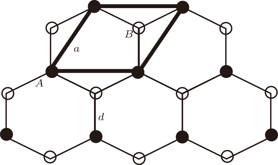 | Fig. 1. Crystal structure of silicene. The lattice is hexagonal, a unit cell is indicated, and the basis consists of two Si atoms labelled A and B. |
Typical structural parameters are given in Table 1 and compared to a classical MD calculation. The out-of-plane height Δ z of the Si atom was found to be 0.44 Å by Cahangirov et al.[27] and 0.45 Å by us.[18] In bulk Si, the out-of-plane Si atom is 0.78 Å from the (111) plane. Thus, the bonding in silicene can be viewed as in between sp2 and sp3. The bond length d is much larger than that for graphene because of the larger size of silicon compared to carbon. A variety of tests showed the low-buckled (LB) structure to be stable. Thus, the LB structure was found to be preserved upon performing ab initio MD on a (4× 4) supercell with temperature as high as 1000 K. Also, the phonon spectrum only has positive frequencies. We note that the classical MD calculations do not reproduce the lattice parameters accurately. In another case, a recent Monte Carlo calculation using the Tersoff potential did not find any buckling, [28] contrary to all the DFT calculations.
| Table 1. Structural parameters of silicene compared to graphene and silicon. |
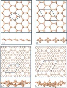
The above structural optimization assumed a hexagonal cell, clearly a very restrictive assumption. More general optimization has revealed that other structures might have lower energies. Kaltsas and Tsetseris[29] started with different configurations by taking the surface layer of various Si surface reconstructions and optimizing the structure. They found that structures based on the 
 | Fig. 2. Possible stable forms of silicon monolayers: (a) silicene, (b)  |
The interest in silicene and graphene is due to the presence of valence and conduction bands with linear dispersions, so-called Dirac cones, crossing at the Fermi energy and at the K and K′ points (in the absence of spin– orbit coupling) in the hexagonal Brillouin zone. The Dirac cones form valleys in the Brillouin zone and the two degenerate bands at a given point originate from the A and B sublattices of the hexagonal structure. For graphene, these Dirac bands originate from the pz states on each sublattice; these states are decoupled from the other s and px, py states due to the reflection symmetry in the graphene plane. In a TB calculation, the Hamiltonian is of order two and the Dirac bands can be related to pseudospins.
For silicene, due to the lack of mirror symmetry, pz states are coupled to px and py states, as well as s states. A minimal TB basis then requires at least eight orbitals and the π and σ bands are coupled. The earliest band structure of silicene was calculated using DFT in 1994 though the presence of Dirac cones was not realized.[4] The fact that a linear dispersion is present was argued for on the basis of symmetry by us in 2007 and also shown to occur by solving analytically the TB Hamiltonian.[1] Two example TB band structures obtained are shown in Fig. 3. It is clear that the exact band structure is heavily dependent upon the exact TB model used, one of the shortcomings of the TB method. Nonetheless, the Dirac point is exactly reproduced in both models.
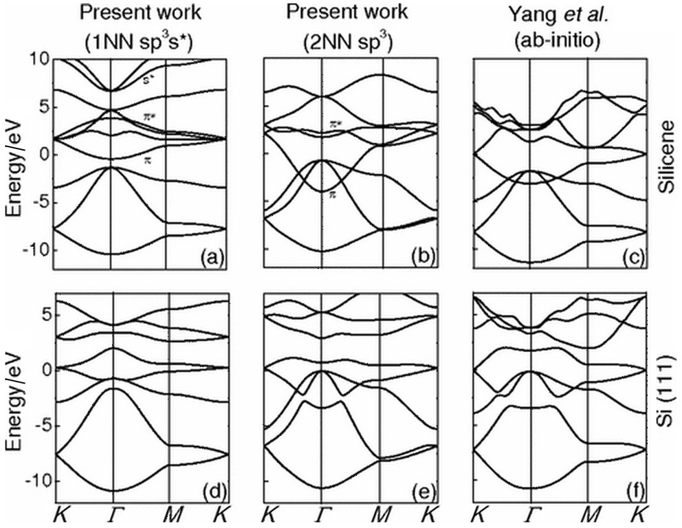 | Fig. 3. Band structure of flat silicene (labeled silicene in the figure) and buckled silicene (labeled Si (111)) using TB models (left two sets of figures) compared to an ab initio calculation[6] (right two figures). Reprinted figure with permission from Guzmá n-Verri and Lew Yan Voon, 2007, Phys. Rev. B76 075131. Copyright (2007) by the American Physical Society. |
While the Dirac cones have been observed for graphene, it remains a prediction for free-standing silicene[1] and whether it is present for silicene on silver remains a controversy[30– 38] in spite of early claims of observation.[15, 39, 40]
Spin– orbit coupling of bands usually removes degeneracies. Inclusion of the latter effect has been shown to open a small gap of 1.55 meV for silicene (while it is negligible for graphene) and, therefore, might be better than graphene at displaying the quantum spin Hall effect (QSHE).[41]
k· p has also been used to study the band structure of silicene[24, 42] and graphene. This model provides semi-analytical results, is more efficient than either TB or DFT, and provides a physical picture. Most treatment to date have been restricted to the linear approximation near the K point. For example, in the presence of spin– orbit coupling, one has[43, 44]

where η = ± 1 for the two valleys K and K′ , σ z are the Pauli matrices associated with the electron spin, τ z are the Pauli matrices associated with pseudospin, and the Rashba term (last term) is present due to inversion asymmetry.
However, the use of symmetry allows one to write down the most general Hamiltonian for silicene. First of all, we note that, in the absence of spin– orbit interaction, all bands are at most doubly degenerate.[24] To leading orders and in the presence of strain ɛ , electric field E, and magnetic field B but without spin– orbit coupling, [24] one can write


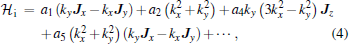


with higher-order terms neglected. The coefficients ai’ s, bi’ s, ci’ s, and ei’ s are the so-called k· p parameters. The Hi terms form the Hamiltonian of the intrinsic band structure while the other ones exist in the presence of external fields. The Ji matrices, if present, represent the pseudospin degree of freedom and are the (2× 2) Pauli pseudospin matrices. The bands giving rise to the Dirac cones are known to be two-fold degenerate at the K point.
When the Hamiltonian is diagonalized, the a1 and a2 terms provide quadratic in k contributions while the a4 and a5 are of cubic order but only the a4 term gives rise to an anisotropic term. Hence, one can readily see that the band structure of silicene is isotropic to linear and quadratic orders and anisotropic effects only manifest themselves if cubic terms become important. For comparison, the corresponding intrinsic Hamiltonian for graphene[45] is

and the anisotropic term is quadratic in the wave vector. The difference is purely due to the buckled geometry of silicene compared to the flat geometry of graphene. Hence, these k· p models of the band structure of these materials reveal their intrinsic differences that might not be evident from a DFT calculation.
The slope of the linear bands, known as the Fermi velocity, is an important parameter. For example, it was recently used in understanding the transistor action of the first ever silicene-based FET.[16] Using DFT, Cahangirov et al.[27] estimated them to be ∼ 106 m/s for silicene, about the same value as for graphene. However, we, [1] using TB models, evaluated them to be ∼ 105 m/s for silicene. Dzade et al.[46] also obtained a smaller Fermi velocity for silicene. That this is so can be easily understood from the reduced hopping in silicene since the Si atoms are more distant from each other than the carbon atoms are in graphene.
An understanding of strain effects on the band structure of silicene is important because the latter might be grown on a substrate with a different lattice constant or strain is often viewed as a way to generate a different band gap in a semiconductor. Calculations of a free-standing silicene sheet under strain have been carried out using DFT.[47– 57] In all cases, the unstrained relaxed structure is first obtained and then the unit cell is distorted in the appropriate direction such that the strain in that direction is given by

where a0 (a) is the equilibrium (strained) lattice parameter. Since the symmetry is reduced for a uniaxial strain, it is convenient to use a rectangular 1× 2 supercell with four atoms.
Considering first a biaxial strain, a biaxial tensile strain was found to lead to a semimetal– metal transition when the strain is larger than 7%.[47, 48, 50, 51] This is due to the lowering of the conduction band at the Γ point; the Dirac point was also found to increase in energy (but remaining degenerate), [48] leading to the possibility of p-type self-doping.[50] On the other hand, a biaxial compressive strain leads to a lowering of the Dirac point below the Fermi level, leading to n-type doping.[51] The Fermi velocity is found to decrease slowly with strain, decreasing to 94% of the unstrained value for strain up to 7%.[48]
A uniaxial strain is expected to lead to a gap opening due to the symmetry lowering. A gap was reported to open up for uniaxial tensile strain, up to 0.08 eV for strain along the zigzag (ZZ) direction and up to 0.04 eV for strain along the armchair (AC) direction, [49] at about 8% and 5%, respectively.
Mohan et al.[53] also obtained a small band gap for tensile strain but found that a direct band-gap of 389 meV is formed for 6% uniaxial compression. However, Qin et al.[54] and Yang et al.[57] did not obtain a gap under a uniaxial strain and only obtained the Dirac point to shift. This controversy has been resolved by our recent application of k· p theory.[24] We have confirmed the lack of a band-gap opening; from Eq. (5), it can be seen that both bands at the Dirac point have the same defomation potential, which means they would both be affected equally by the strain. Qin et al. did obtain a dependence of the Fermi velocity with the type of uniaxial strain as well as a wave-vector dependence; this is consistent with the k· p theory since the bands are no longer degenerate away from the K point and would be governed by different deformation potentials.
 | Fig. 4. Band gap with uniaxial tensile strain for silicene. Reprinted from Phys. Lett. A, 376, Huijuan Zhao, Strain and chirality effects on the mechanical and electronic properties of silicene and silicane under uniaxial tension, page No. 3546, Copyright (2012), with permission from Elsevier.[49] |
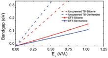
Electric field effects on silicene are important because, contrary to graphene, a perpendicular electric field is predicted to lead to a gap opening.[58– 60] This can be easily understood in terms of the two atoms in a unit cell experiencing different electrostatic potentials since they are at different heights. The field also has an effect on the buckling parameter; the vertical electric field was found to increase the buckling parameter quadratically with the field.[58]
Ni et al.[58] found that a vertical electric field opened a band gap in single layer silicene, and the gap increased linearly with the field up to about 1 V/Å (Fig. 5). The linear dependence agrees with our k· p theory, Eq. (6), which also predicts a quadratic dependence for larger fields and a quadratic response for an in-plane electric field. Ni et al. obtained a rate of 0.157 eÅ while Drummond et al.[59] got 0.0742 eÅ . The latter also indicated that the gap actually starts closing for E⊥ ≈ 0.5 V· Å − 1 due to the overlap of the conduction band at Γ and the valence band at the K point. The electric field leads to an almost linear increase in the effective mass; for example, for a field of 0.4 V/Å , the hole mass was found to be 0.015m0 (0.033m0) along the KΓ (MK) direction and about 2% different for the electron mass.
 | Fig. 5. Band gap change with perpendicular electric field. Reprinted with permission from Ni et al., Nano Lett.12(1), 113 (2012). Copyright (2012) American Chemical Society. |
Silicene is a Kane– Mele-type 2D topological insulator (TI).[61] A TI has a bulk energy gap but gapless edge states that allow correlated charge and spin transport (Fig. 6). It can be distinguished from the more common band insulator (BI) because the charge transport is protected from disorder (due to the correlation with spin) and, mathematically, this can be represented by a different topological order or quantum number, the Z2 invariant.[63] There are two topological quantum numbers: the Chern number C and the Z2 index; the latter is also the same as the spin-Chern number Cs when the spin σ z is a good quantum number. Qualitatively, this is so far not different from graphene. Indeed, Liu et al.[41] used the fact that the Hamiltonian of the buckled structure can be continuously obtained from the flat one (an explicit TB Hamiltonian illustrating this process had been provided by us[1]) to demonstrate the quantum spin Hall (QSH) state for silicene. The QSH of the TI is generated with the assistance of the spin– orbit coupling. The larger spin– orbit coupling gap of 1.55 meV[41] for silicene makes it more practical than graphene for realizing a TI.
 | Fig. 6. One-dimensional energy bands for a silicene nanoribbon. (a) The bands crossing the gap represent edge states (topological insulator). (b) All states are gapped (band insulator). Reproduced from Ref. [62] with kind permission from Springer Science and Business Media. |
The topological properties for silicene would be different from graphene in the presence of an external electric field since the buckled structure of silicene leads to a gap opening. In fact, the interplay of the spin– orbit gap and an electric field induced gap allows for a transition between a TI and a BI (where the gapless edge states are not protected by topology). This quantum phase transition was computed to occur for a vertical field of 20 mV/Å .[59] Additionally, this is accompanied by a transition from the QSHE to the quantum valley Hall effect (QVHE).[64, 65] In the presence of an exchange field M and an electric field Ez, one can plot a phase diagram (Fig. 7). Ezawa computed four principal phases:[62] band insulator (BI), quantum anomalous Hall (QAH), quantum spin Hall (QSH), valley-polarized metal (VPM), and spin valley-polarized metal (SVPM). The QAH is characterized by an insulating bulk gap and chiral gapless edges; it is induced by the internal magnetization and by the spin– orbit coupling, i.e., it displays quantized Hall conductance in the absence of an external magnetic field. The valley-polarized metal refers to silicene with electrons moved from the conduction band at K to the valence band at K′ in a perpendicular electric field. Ezawa has further exploited the buckled structure of silicene to postulate additional topological phases not encountered for graphene. Thus, an inhomogeneous electric field is shown to generate a helical zero mode away from the edges by closing the band gap spatially, [66] while circularly polarized light was used to trigger a topological phase transition from one TI to another TI as a result of the photon dressing of the bands.[67] It was also postulated to break the valley degeneracy by introducing different exchange fields on the two sublattices[44] leading to such states as a QSQAH one (with one valley being a QSH state and the other being a QAH one) and single-valley semimetals (one valley is closed, the other is open). This ability to control the K and K′ valleys independently is termed
 | Fig. 7. Phase diagram for silicene in exchange field M and electric field Ez. The insulator phases are indexed by the Chern and spin-Chern numbers (C, Cs). Reprinted figure with permission from M. Ezawa, 2012 Phys. Rev. Lett.109 055502. Copyright (2012) by the American Physical Society. |
valleytronics. The different exchange field could be generated by adsorbing different tranition metal atoms to the two sublattices or by sandwiching the silicene between two different ferromagnets. The valley-selective band structure can be probed by using circularly-polarized light leading to circular dichroism. A complete tabulation of the topological indices for the various phases in silicene is provided in Ref. [68].
The fundamental electronic properties of silicene have been reviewed, with particular emphasis on those that could be elucidated by the use of empirical band structure models such as tight binding and k· p. Similarities and differences to graphene have been pointed out. Similarities include the presence of Dirac cones for both materials. Differences in the intrinsic Hamiltonian occur at a higher order then linear but they occur at the linear level with an external electric field. k· p theory is shown to clarify the rather non-intuitive result that a uniaxial strain does not open a band gap for silicene.
Lok Lew Yan Voon acknowledges the support of the Traubert Chair and of The Citadel Foundation.
| 1 |
|
| 2 |
|
| 3 |
|
| 4 |
|
| 5 |
|
| 6 |
|
| 7 |
|
| 8 |
|
| 9 |
|
| 10 |
|
| 11 |
|
| 12 |
|
| 13 |
|
| 14 |
|
| 15 |
|
| 16 |
|
| 17 |
|
| 18 |
|
| 19 |
|
| 20 |
|
| 21 |
|
| 22 |
|
| 23 |
|
| 24 |
|
| 25 |
|
| 26 |
|
| 27 |
|
| 28 |
|
| 29 |
|
| 30 |
|
| 31 |
|
| 32 |
|
| 33 |
|
| 34 |
|
| 35 |
|
| 36 |
|
| 37 |
|
| 38 |
|
| 39 |
|
| 40 |
|
| 41 |
|
| 42 |
|
| 43 |
|
| 44 |
|
| 45 |
|
| 46 |
|
| 47 |
|
| 48 |
|
| 49 |
|
| 50 |
|
| 51 |
|
| 52 |
|
| 53 |
|
| 54 |
|
| 55 |
|
| 56 |
|
| 57 |
|
| 58 |
|
| 59 |
|
| 60 |
|
| 61 |
|
| 62 |
|
| 63 |
|
| 64 |
|
| 65 |
|
| 66 |
|
| 67 |
|
| 68 |
|