


Silicene on substrates: A theoretical perspective
[Zhong Hong-Xiaa), c) † , Quhe Ru-Gea), d), e), f) † , Wang Yang-Yanga), g) † , Shi Jun-Jiea) , Lü Jing†‡a), b)  ]
]
]
|
|


†These authors contributed equally to this work.
‡Corresponding author. E-mail: jinglu@pku.edu.cn
*Project supported by the National Natural Science Foundation of China (Grant Nos. 11274016 and 11474012), the National Basic Research Program of China (Grant Nos. 2013CB932604 and 2012CB619304), and the National Natural Science Foundation of China (Grant No. 1207141).
Silicene, as the silicon analog of graphene, is successfully fabricated by epitaxially growing it on various substrates. Like free-standing graphene, free-standing silicene possesses a honeycomb structure and Dirac-cone-shaped energy band, resulting in many fascinating properties such as high carrier mobility, quantum spin Hall effect, quantum anomalous Hall effect, and quantum valley Hall effect. The existence of the honeycomb crystal structure and the Dirac cone of silicene is crucial for observation of its intrinsic properties. In this review, we systematically discuss the substrate effects on the atomic structure and electronic properties of silicene from a theoretical point of view, especially with emphasis on the changes of the Dirac cone.
As the silicon analogy of graphene, silicene possesses graphene’ s both outstanding properties like the Dirac-cone-shaped energy band[1] and the high carrier mobility: theoretically each of silicene and graphene has a carrier mobility on the order of 103 cm2/(V· s)– 105 cm2/(V· s), [2, 3] and undesirable zero band gap nature.[1] Unlike planar graphene, whose band gap is difficult to open without degrading its electronic property, [4] silicene has a tunable band gap that can be opened in low-buckled silicene (0.44 Å ) by a vertical electric field, [5, 6] single-side surface adsorption of alkali and transition metal atoms without degrading the electronic properties of silicene.[7, 8] Meanwhile, three (p/i/n) doping types are realized for silicene sheets, which can be used to fabricate silicene-based p– i– n transport field effect transistors (FETs).[8] Because of the high carrier mobility, a tunable band gap, and easy integration into the modern Si-base device technologies, silicene is a promising material for high-speed electronic devices, and the silicene-based transistor will own an extremely fast speed, making it able to operate in the THz frequency range.[9] Very recently, a silicene FET operating at room temperature has been realized via growth-transfer-fabrication process, corroborating the expected ambipolar Dirac charge transport.[10]
Due to the stronger spin– orbital coupling (SOC) of Si atom than that of C atom, silicene with an SOC band gap about 1.55 meV (24× 10− 3 meV in graphene)[11] is more eligible in realizing quantum spin Hall effect (QSHE) and fabricating spintronics devices.[12] By adjusting an electric field and/or an exchange field, the QSHE, quantum anomalous Hall effects (QAHE) and valley-polarized QAHE, the quantum valley Hall effect (QVHE), and the valley polarized metal (VPM) state can be realized in silicene, [13, 14] providing many potential applications in spintronics and valleytronics. Based on these topological states, spin-filters and spin/valley separators with quite good performance are designed.[15] Therefore silicene serves as an ideal platform for efficiently manipulating spin/valley degrees of freedom.
Unfortunately, silicene is much less stable and more difficult to synthesis than graphene. As is well known that graphene, with sp2-bonded carbon atoms, can be exfoliated from graphite easily because of the weak van der Waals (vdW) interlayer interactions of graphite. However, silicene, a low-buckled structure with partial sp3-bonded silicon atoms, cannot be exfoliated from bulk silicon due to the strong covalent Si– Si bonds. Thus, the exfoliation technique developed for graphene does not work for silicene. Hence the major method of synthesizing silicene sheet is to epitaxially growing it on solid surfaces. Silicene has been first successfully synthesized by depositing silicon onto Ag (111) substrate, [16, 17] and further obtained by segregation on the top of ZrB2 thin film epitaxially grown on Si wafer, [18] and then by directly depositing silicon atoms onto Ir (111) surface and annealing the sample at 670 K, [19] and being deposited on the ZrC (111) at 800 K.[20] Recently, high-buckled two-dimensional (2D) Si nanosheets (2 Å in thickness) has been fabricated by molecular beam epitaxial growth on bulk MoS2 surface.[21] Many other substrates, including graphene, Ca, Pb, SiC, BN, MoX2 (X = S, Se, and Te), WSe2, and GaS, have been proposed and investigated theoretically.[22– 27]
In order to observe the high carrier mobility and various topological properties, the honeycomb crystal structure and the Dirac cone of silicene must be maintained. Therefore, the effects of the substrates on the structural and electronic properties of silicene must be clarified. In this review, we will discuss the properties of silicene on various substrates. Special attention will be paid to whether the key Dirac cone of free-standing silicene can be preserved on substrate. The reviewed substrates generally satisfy two criteria: hexagonal symmetry lattice and a small lattice mismatch (Δ a) with silicene. This review is organized into the corresponding two sections as follows. In the first section, we discuss the electronic properties of epitaxial silicene layers on Ag, ZrB2 (ZrC), Ir, and other metallic substrates. Due to enhanced band hybridization, the absence of the Dirac cone is a common characteristic for silicene on metal substrates, except for graphene, Ca, and Pb. On these three metal surfaces, supported-silicene can preserve its intrinsic Dirac cone below the Fermi level (Ef). In the second section, silicene layers on insulating and semiconducting 2D layered substrates, including SiC, BN, MoX2 (X = S, Se, and Te), WSe2, GaS, and other non-metallic substrates are summarized. It is found that the lattice mismatch and work function play crucial roles in the electronic properties of silicene on non-metallic substrates.
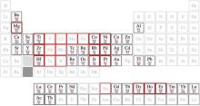
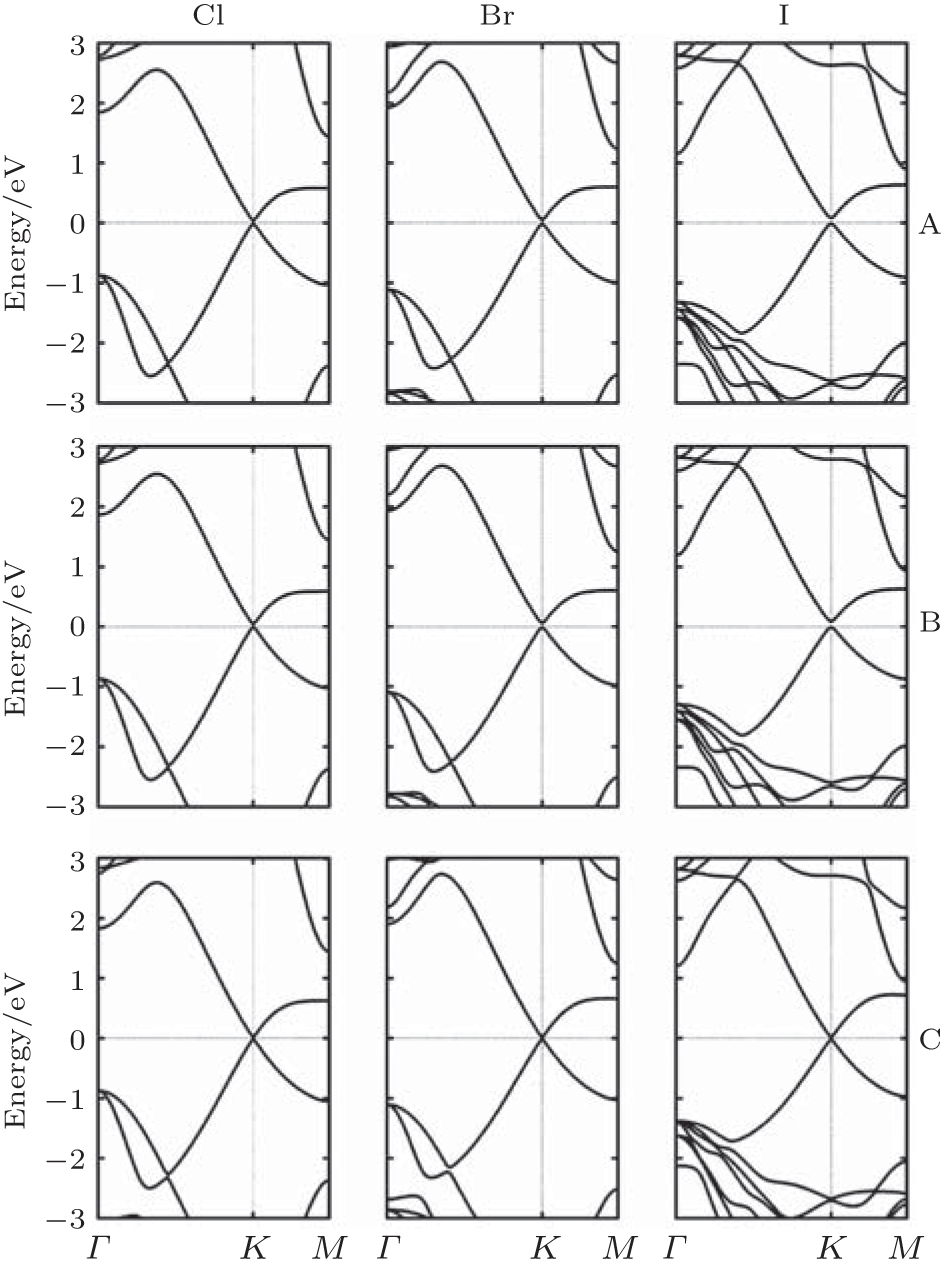
Because silicene does not exist in nature, we must evaporate and deposit Si atoms on substrates (or templates) to synthesize it. The major method of synthesizing silicene is to epitaxially growing it on metallic substrates, and this method has been used up to now. For instance, silicene has been successfully grown on metallic Ag, ZrB2, [18] Ir, [19] and ZrC[20] substrates. Additionally, silicene must contact metal electrodes in real device applications. Understanding the nature of silicene on metallic surface will pave a way for investigating other important physical phenomena such as superconductivity.[28– 30] Many efforts thus have been devoted to both theoretical and experimental researches of silicene on metals. According to the periodic table, we focus on the researches of fcc metals with (111) surfaces and hcp metals with (0001) surfaces because of their hexagonal symmetry, which are indicated by brightness in Fig. 1.[22]
 | Fig. 1. Periodic table. The metals with fcc and hexagonal structure are indicated. The corresponding (111) or (0001) surfaces have hexagonal symmetry. The crystal structure is indicated (in red), while the relative lateral lattice constant compared with that of silicene is given as a (blue) number in per cent. The elements in red squares form silicides. Reproduced with permission from Ref. [22] (Copyright 2014 Institute of Physics). |
Among all the metallic substrates, Ag is the most common substrate to synthesis silicene experimentally because of the moderate and homogeneous interaction, and good lattice match between Ag (111) surface and silicene.[31] Several phases of silicene have been successfully fabricated by epitaxial growth on Ag (111) with superstructures of
(3× 3)silicene/(4× 4)Ag (111), [16, 32– 35]
(2× 2)silicene/


and 
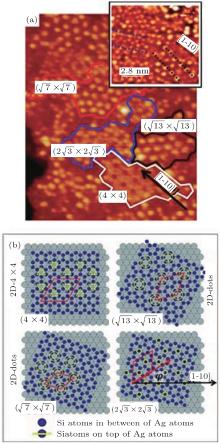
 | Fig. 2. STM characterization of multi-oriented silicene domains on Ag (111). (a) From an STM image, a pictorial view of individual Si domains with patch together to form a larger interconnected sheet. In the inset a different STM image (V = − 1.5 V, I = 0.2 nA) emphasizes the different orientations of the patterned silicene domains; the black arrow indicates the [1– 10] direction of the Ag (111) surface, while dotted guidelines (red, blue, and black) distinguish the different preferential orientations of the silicene superstructures. (b) Sequence of ball models which simulate the superpositions of oriented honeycomb silicene lattices (blue spots) on the Ag (111) surface (grey spots); several superstructures are generated by particular orientations of the silicene with respect to the Ag (111) lattice (Reproduced with permission from Ref. [32]. Copyright 2012 Wiley Online Library). |
The appearing of different superstructures is attributed to the different substrate temperatures and deposition rates.[35] Among these different superstructures, the phase of (3× 3)silicene/(4× 4)Ag (111) has attracted most attention due to the small Δ a (0.3%). Experimentally, there is a fierce debate over the existence of Dirac cone in silicene on Ag surface. The scanning tunneling microscope (STM) and angle-resolved photoemission spectroscopy (ARPES) results in phases (3× 3)silicene/(4× 4)Ag (111), which provide an evidence that both structural and electronic properties of the 2D silicene are very similar to those of graphene.[37] Unfortunately, the scanning tunneling spectra (STS) in
(3× 3)silicene/(4× 4) Ag (111) and


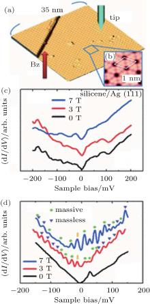
 | Fig. 3. (a) STM image of large area of silicene (sample bias voltageVs = 0.70 V and tunneling current It= 0.19 nA. The image size is 35 nm× 35 nm). (b) High resolution STM image of the 4× 4 silicene (Vs = + 0.50 V and It= 0.30 nA, 3.65 nm× 3.65 nm). The unit cell is shown by the white rhombus. (c) The STS spectra of silicene for various magnetic fields perpendicular to the sample surface, Bz. (d) The STS spectra of HOPG for various values of Bz. The purple triangles and green circles show the peaks originating from the LLs of massless and massive Dirac fermions, respectively. The n = 0 LL is marked by the yellow bar and the n = 1 LL of massive Dirac fermions is not clearly resolved in 3 T due to low magnetic field (Reproduced with permission from Ref. [33]. Copyright 2013 American Physical Society). |
Subsequently, extensive theoretical calculations clarify that the Dirac cone in the observed phases of
(3× 3)silicene/(4× 4)Ag (111),
(2× 2)silicene/


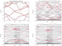
 | Fig. 4. (a) Free-standing silicene band structure, in which the π and π * bands degenerate at Ef. (b) and (c) Projected band structures of silicene/Ag (111) composite systems. Red dots and gray dots represent the states contributed by Ag and Si atoms, respectively. The intensity of the color is proportional to the weight of the corresponding atoms. Black squares indicate those states probably contributed from the π (π * ) bands of silicene. Ef is set to be zero. (For the further implications of color in this figure, the readers can refer to the web version of this article) (Reproduced with permission from Ref. [40]. Copyright 2014 North-Holland). |
 | Fig. 5. (a) Bands of reconstructed (3× 3) silicene in the absence of Ag substrate (unsupported silicene) unfolded to BZ of (1× 1) silicene, shown by red dots. The radii of dots correspond to the weight of unfolding. The band structure of ideally buckled silicene is shown by green lines. (b) Unfolded band structure of silicene on Ag. Red dots refer to states with significant contribution from silicene (Reproduced with permission from Ref. [39]. Copyright 2013 American Physical Society). |
The situation becomes more complicated for the newly found phase of 


Although it is controversial whether the Dirac cone is present for Ag-supported silicene in experiments, most theoretical calculations reach the consistent conclusion that the Dirac cones of all Ag-supported silicene are severely destroyed by the strong band hybridization between silicene and Ag substrates from the electronic band structure. In Table 1, we present the theoretical structural parameters of hybrid structures, such as supported-silicene buckling (Δ ), the vertical distance from the bottom silicene layer to the topmost metal layer (d0), binding energy (Eb) (per Si atom) required to remove the silicene sheet from the surface, and charge transfer (Q). The various phases of Ag-supported silicene display large Δ of 0.95 Å ∼ 1.65 Å , small d ranging from 1.23 Å ∼ 1.87 Å , Eb of 0.7 eV, and Q of − 0.07| e| .[40, 46, 49]
| Table 1. Structure parameters of the silicene on various metallic substrates. a is the lattice constants of materials, Δ a is the lattice mismatch between substrates and free-standing silicone, Δ is the calculated buckling of metal supported-silicene, d0 is the equilibrium separation of silicene from various surfaces, Eb is the binding energy (per Si atom) required to remove the silicene sheet from the surface, W is the work function for the clean metal surface, Q is the Mulliken charge per Si atom transferred from silicene to the metal surfaces. In the last column, Yes (No) denotes the existence (absence) of the Dirac cone of silicene. The lattice constant, low (high) buckling, and work function of free-standing silicene are 3.87 Å , 0.44 (2.00) Å , and 4.48 eV, respectively. |
With high melting point, high hardness, high stability against oxidation, and high electric conductivity, the transition-metal carbides (TMCs) and diborides belong to a group of compounds, which have promising applications to high-temperature ceramics and are highly stable substrates for film growth. Fleurence et al. successfully synthesized the phase 


Silicene has been successfully fabricated on Ir (111) surface by directly depositing silicon on the Ir (111) surface and annealing the sample at 670 K.[19] Both theories and experiments verify the 2D continuity and buckled structure of silicene on Ir (111).[19, 52] The phase 

Owing to the hexagonal symmetry and similar honeycomb lattice constants, the heterosystem silicene/graphene is reasonable to have no imaginary phonon frequency.[27, 53– 55] Multiple phases of silicene with different orientations relative to graphene have been calculated with small Δ a (0.5%∼ 2.7%).[27] From among the various phases, we take the phase 


Like the phase 

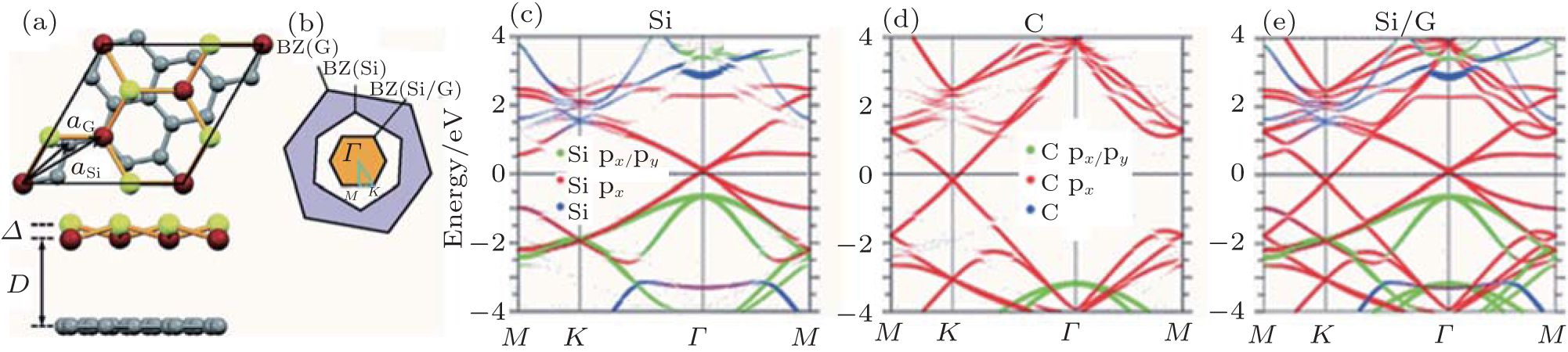 | Fig. 6. (a) Top and side views of the atomic structure of     |
The cases of silicene on other promising metals have been predicated theoretically, including


(1× 1)silicene/Ca (111),


(3× 3)silicene/
(2× 2)silicene/(3× 3)Ru (0001),
(4× 4) silicene/(6× 6)Rh (111),
(3× 3)silicene/


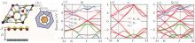
Now we first come to discuss the case of silicene on Ca (111) with Δ a smaller than 1.5%.[22] Among them, the calculated STM images clearly demonstrates the perfect honeycomb symmetry of silicene on 1× 1 Ca (111), and a functionalized Ca(1.0 ML)/(1× 1) Si (111), accompanied by Δ values of 0.72 Å and 0.69 Å , respectively. Moreover, the Si pz-state derived Dirac cones could be identified near the K point for these two substrates as shown in Fig. 7, with corresponding Fermi velocity on the order of 105 m/s. Furthermore, band gaps (574 meV and 161 meV) at the Dirac point appear, and the Dirac point is shifted by more than 0.5 eV below Ef.
The other promising metallic substrate to grow and host Dirac fermions is Pb (111) surface, due to its chemical stability to Si and its threefold symmetry.[23] Three silicene superstructures are studied with Δ a no greater than 3.0%. The honeycomb structure of silicene is maintained in all cases, with equivalent Δ of 0.65 Å ∼ 0.74 Å , higher d0 (2.8 Å ), lower Eb (0.15 eV), and Q (0.05| e| ) compared with those for the case of silicene/Ag (111). Consequently, the band structures of the silicene superstructures in Fig. 8 clearly show the original cone-shaped band structures of free-standing
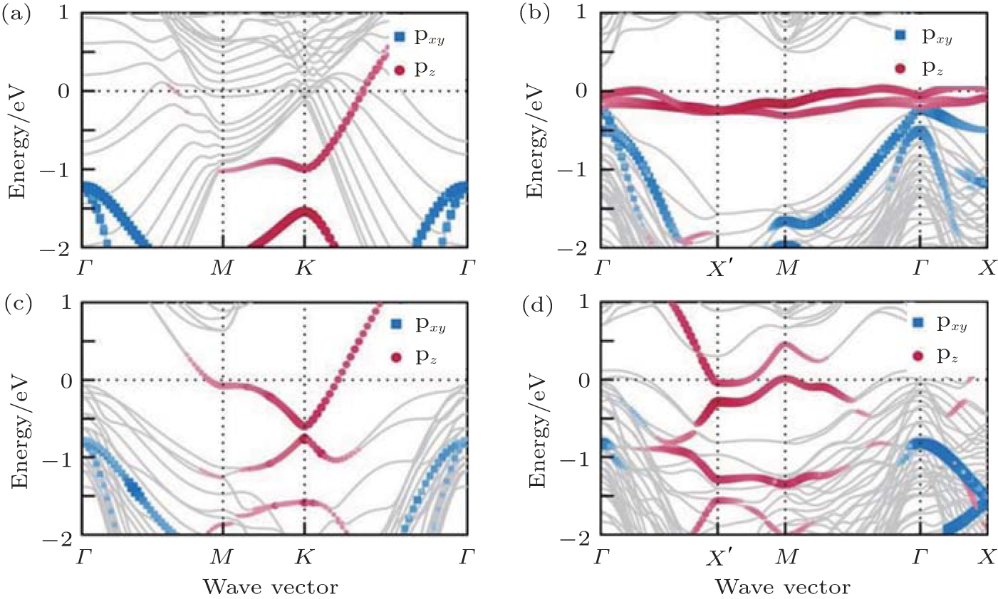 | Fig. 7. Band structures of silicene on (a) Ca (111) 1× 1, (b) Ca(0.5 ML)/Si (111) 2× 1, (c) Ca(1.0 ML)/Si(111) 1× 1, and (d) Ca(1.5 ML)/Si (111) 2× 1 surfaces. The silicene pz (silicene pxy) characteristic of the bands is indicated by red dots (blue squares) of varying size. All bands without silicene characteristics are given by grey lines (Reproduced with permission from Ref. [22]. Copyright 2014 Institute of Physics). |
 | Fig. 8. Band structures of the silicene superstructures (a)   |
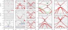
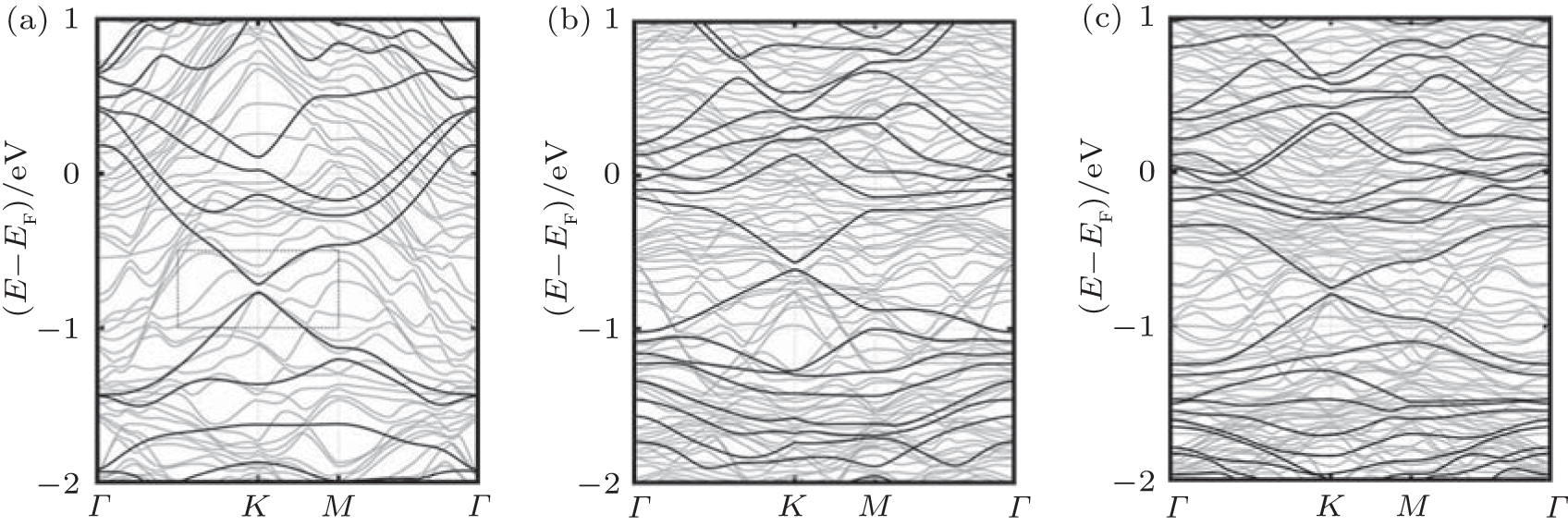
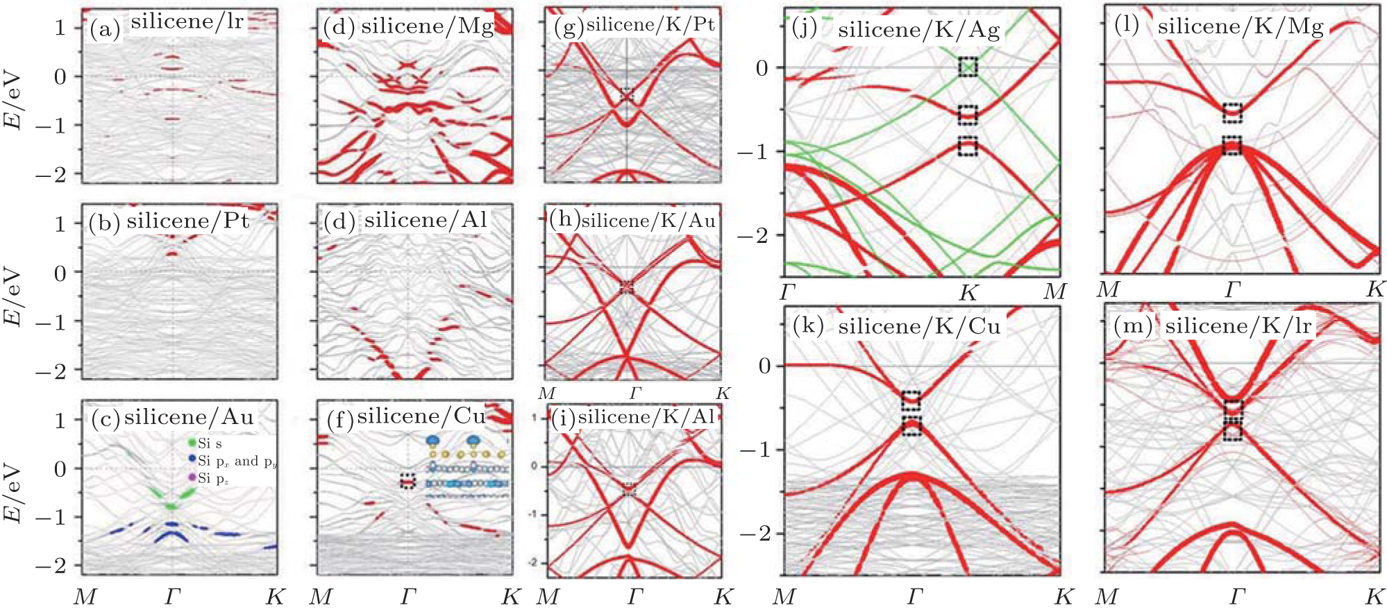
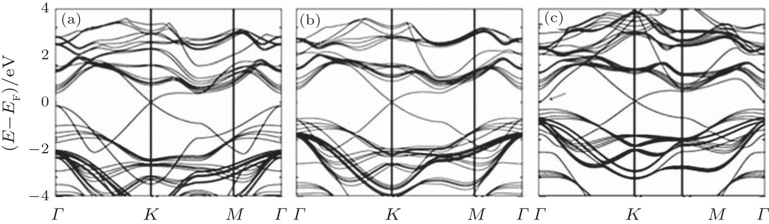
Except for Ca and Pb metals, the severe destruction of the silicene original Dirac cone due to the strong band hybridization between silicene and metallic substrates appears to be a common characteristics for metal supported-silicene as shown in Figs. 4 and 9(a)– 9(f)[40, 46] Fortunately, the destroyed Dirac cone can be restored by intercalating low concentration alkali metal atoms between silicene and substrates.[46] After intercalating K atoms for silicene on Pt, Au, and Al surfaces, the Si atoms are almost in the same plane (Δ = 0 Å ), and the zero Dirac cone is well recovered, with the estimated Fermi velocity on the order of 105 m/s, because of the recovered inversion symmetry of no buckling silicene (Figs. 9(g)– 9(i)). While for the cases of silicene, with the intercalating of K atoms, on Ag, Mg, Cu, and Ir surfaces, the recovered Dirac cone is located at 0.40 eV∼ 0.78 eV below Ef, with an opened band gap of 0.15 eV∼ 0.40 eV, due to the built-in electric field induced by charge transfer (Figs. 9(j)– 9(m)).
Devices of silicene require non-metallic substrates. Therefore, identifying non-metallic substrates suitable to host silicene is an important issue for realizing the devices based on silicene. We focus on a layered material with a honeycomb structure, such as insulating SiC and BN, transition-metal dichalcogenides MoX2 and GaX (X = S, Se, Te), which are held together by weak vdW. The choice of these hexagonal layered templates for silicene is motivated by the following factors: (i) considerable band gaps (1 eV– 6 eV); (ii) small lattice mismatch between silicene layer and substrates; (iii) pristine surfaces without out-of-plane dangling bonds, which may predict a weak interaction between silicene sheet and substrates.
 | Fig. 9. (a)– (f) Band structures of epitaxial  |
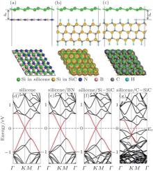
Recent first principles calculations proposed that the outstanding properties like the Dirac cone of silicene should be retained on hexagonal ML boron nitride (h-BN) and hydrogenated SiC (0001) surface.[6, 24] The phases of (2× 2)silicene/(3× 3)BN and (4× 4)silicene/(5× 5)SiC (0001) are constructed because of their small Δ a values of 2.04% and 0.08%, respectively. The honeycomb structure of silicene is maintained with a large d0 (about 3 Å ) on insulating BN and SiC substrates as shown in Fig. 10. This d0 is comparable to that for graphene/BN system (3.22 Å ) and is larger than that for silicene/metals. This large d0 leads to a small Eb of 0.07 eV∼ 0.09 eV, indicating that the interaction between silicene and substrates is rather weak and can be viewed as vdW type. The weak vdW interaction results in small Δ of about 0.50 Å for silicene on BN and SiC, which is very close to the free-standing silicene buckling (0.44 Å ). Therefore, the Dirac cones of silicene can be highly expected to be on these insulating hexagonal templates.
Furthermore, the original linear dispersion band of silicene is clearly preserved on the ML h-BN and Si-terminated SiC (0001) surface as shown in Figs. 10(e) and 10(f). It must be noted that the gapped Dirac cone is nearly at Ef (without any doping) in the band gaps of the two insulating substrates.[24, 56] By contrast, for the silicene/C– SiC system, the supported-silicene becomes metallic, with the lower segment of the Dirac cone mixing up with the valence bands of the substrate in Fig. 10(g). The difference in band structures between these combined systems is also verified by the partial charge densities analyses, which concentrate on silicene near Ef for silicene/BN and silicene/Si– SiC, but distribute widely into the substrates for silicene/C– SiC.
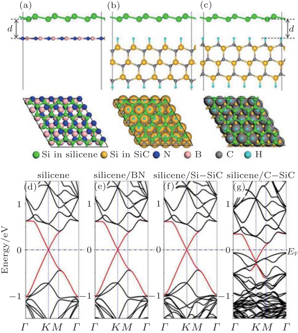 | Fig. 10. Side (upper) and top (lower) views of the atomic configurations of (a) silicene/BN, (b) silicene/Si– SiC, (c) silicene/C– SiC hybrid systems. The corresponding electronic band structures of (d) silicene, (e) silicene/BN, (f) silicene/Si– SiC, (g) silicene/C– SiC. The red lines refer to the π -bands of silicene in different configurations (Reproduced with permission from Ref. [24]. Copyright 2013 American Chemical Society). |
The physical mechanisms for the cases in Fig. 10 have been further explored. The different substrate effects are attributed to the different work functions, [24] i.e., the absolute positions of the valence band maximum (VBM) and conduction band minimum (CBM), of the substrates. The CBM (or VBM) of silicene is slightly 0.1 eV lower than the VBM of C– SiC substrate, so that the charge will transfer from C– SiC substrate to silicene. The value of Ef of the hybrid system is thus higher than that of free-standing silicene, and the silicene in the hybrid system becomes metallic. On the contrary, for the silicene/BN and silicene/Si– SiC systems, the CBM of silicene is located in the gap region between BN and Si– SiC, resulting in a little charge transfer between silicene and the substrates. Consequently, the conical point of the Dirac cone in silicene is preserved at Ef, with small opened band gaps of 4 meV on BN and 3 meV on Si– SiC.
Three different possible atomic arrangements of silicene layer (AAA stacking, intermediate position, and ABA stacking) on the top of MoX2 (X = S, Se, Te) have been studied.[25, 57, 58] A large d0 (3.0 Å ∼ 3.5 Å ) and a small Eb (10 meV– 100 meV) suggest that there exists a vdW interaction between silicene and MoX2. As given in Table 2, as Δ a decreases from 18% to 9%, Δ decreases from 1.9 Å for silicene/MoS2 to 0.7 Å for silicene/MoTe2. Thus, the larger the lattice mismatch, the larger the supported-silicene buckling is. Usually, a large buckling suggests that there exists a strong interaction between silicene and substrates, which can enhance the possibility of losing Dirac cone. A large Δ a is unfavorable for silicene epitaxial growth in experiment either.
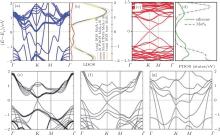
It is noted that Δ of silicene on bulk MoS2 is very close to the value for highly buckled free-standing (2.00 Å ) silicene structure. Highly buckled silicene is predicted to be metallic and has several bands across Ef.[1] The energy band structure and the local density of states (Figs. 11(a) and 11(b)) confirm the metallic nature of silicene on bulk MoS2. The gap of MoS2 substrate is preserved, and all the electronic states near Ef are contributed from Si atoms. This clearly verifies that the vdW type of silicene/MoS2 interaction almost has no hybridization between silicene and substrates. It is noted that the Δ a between 4× 4 silicene and 5× 5 ML MoS2 is rather small (2.42%).[59] In this case, the Δ of silicene on ML MoS2 is 0.56 Å , close to the value for low buckled free-standing silicene structure. The supported-silicene is slightly p-doped and basically maintains its linear energy dispersion as shown in the corresponding electronic band structures and PDOS (Figs. 11(c) and 11(d)). The sublattice symmetry broken induces a small band gap (70 meV) at the Dirac cone. The band gap could be further tuned by an external electric field.
The band analyses are performed for silicene on MoSe2 and MoTe2 in Fig. 11. Interestingly, silicene on bulk MoTe2 in Fig. 11(e) is a zero-gap semiconductor, preserving its Dirac cones at the K point. However, silicene on ML MoTe2 is slightly doped by electrons and becomes metallic (Fig. 11(f)), with the band gap of the Dirac cone slightly opened because the inversion symmetry of silicene is destroyed by the charge transfer between silicene and ML MoTe2.[8, 46] Besides, other energy bands also share the same energy with the Dirac cone. In Fig. 11(g), silicene is moderately doped by electron on bulk MoSe2, with a larger band gap near the Dirac cone. The geometrical structures and electronic structures for silicene on two MoX2 layers in the same atomic configuration are nearly the same as the cases of silicene on ML MoX2.[25]
| Table 2. Structure parameters of the silicene on different non-metallic substrates. Eg is the theoretical band gap of the studied substrates (bulk phase), W is the work function of substrates in ML phase, ED is the band gap near the Dirac cone, and Δ Ef is the energy shift of Dirac cone with respect to Ef. |
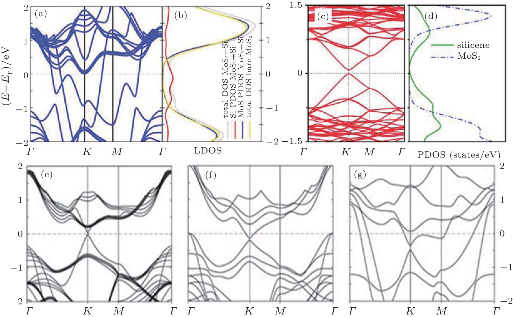 | Fig. 11. Electronic band structure (a) and local density of states (b) of silicene on bulk MoS2. Electronic band structure (c) and partial density of states (d) of silicene on monolayer MoS2. Band structures of silicene on (e) bulk MoTe2, (f) monolayer MoTe2, and (g) MoSe2. Reproduced with permissions from Refs. [25] and [59] (Copyright 2014 Institute of Physics and Royal Society of Chemistry). |
WSe2 has a smallest value of Δ a with silicene (0.6%) among the transition metal dichalcogenides.[26] Because of their instabilities, the combined system varies from metallic state to semiconducting state with a band gap up to 0.3 eV, but accompanied with a well preserved Dirac cone. When WSe2 is doped by S and Te, the combined heterosheet becomes stable, with atomic and electronic structures nearly being the same as those for silicene on pristine WSe2. However, high-buckled silicene on WSe2 has a Δ value of 1.3 Å , a small d0 of 2.55 Å , and a large Eb of 195 meV, indicating strong interaction between silicene and substrates compared with the case of low-buckled silicene (Δ of 0.51 Å , d0 of 3.20 Å , and Eb of 120 meV).
GaX (X = S, Se, Te) is another class of chalcogenide compounds with a vdW layered hexagonal structure. The cell parameters are larger for GaX and the Δ a values (3%∼ 8%) with free-standing silicene are smaller than those for MoX2.[25, 60] A small Eb (0.07 eV) suggests a weak vdW type of silicene/GaX. The Δ values are small, ranging from 0.30 Å ∼ 0.70 Å . The d0 values for silicene on bulk GaX (4.5 Å ∼ 5 Å ) are much larger than those for silicene on ML GaX (3.1 Å ∼ 3.8 Å ), similar to the case of MoX2. It appears that the interaction between the silicene and GaX and MoX2 can be enhanced by reducing the layer number.
 | Fig. 12. Electronic band structures of the silicene layer on (a) bulk GaS, (b) GaSe, and (c) GaTe. The arrow in panel (c) indicates the band crossing Ef (Reproduced with permission from Ref. [25]. Copyright 2014 Institute of Physics). |
Figure 12 displays the electronic band structure of silicene/bulk GaX.[25] Remarkably, both silicene/bulk GaS and silicene/bulk GaSe preserve the linear band dispersion crossing Ef at the K point, with band gaps (0.7 eV and 1.5 eV, respectively) at the Γ point. These two combined systems are expected to be gapless semiconductors, just like free-standing silicene. Therefore, these heterosheets belong to the Dirac system, possessing outstanding properties like the high Fermi velocity and carrier mobility. Although the Dirac cone is preserved for silicene/bulk GaTe, there is a band touching Ef at the Γ point, and this will mask the intrinsic properties of the Dirac carrier. On condition that the sandwiched configurations have the same stacking modes as the bulk structure, there is nearly no difference between ML GaTe/silicene/ML GaTe (silicene in-between two GaTe layers) and silicene/bulk GaTe. The gapless Dirac cone in silicene/bulk GaS turns into a gapped (about 0.1 eV) one in ML GaS/silicene/ML GaS due to the interlayer charge distribution. Furthermore, this gap value of ML GaS/silicene/ML GaS can be modulated by an external electric field and strain.[60]
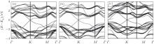
Arranged on hexagonal lattice, ML MgX2 (X = Cl, Br, and I) are insulators with calculated band gaps ranging from 3.6 eV to 6.0 eV.[61] The lattice mismatches between ML MgX2 and silicene are smaller than 2.9%. Three high symmetry configurations of silicene on ML MgX2 (0001) have been checked and turned out to be almost degenerate. All silicene/ML MgX2 heterosheets show small Δ (0.39 Å ∼ 0.55 Å ), large d0 (3.23 Å ∼ 3.75 Å ), and small Eb (33 meV∼ 88 meV), a typical weak vdW interaction. The band structures of silicene on ML MgX2 (0001) for three configurations are displayed in Fig. 13.[61] In each case, the supported-silicene is minor p doping and preserves its intrinsic electronic properties well, such as the Dirac-cone-like energy band and high Fermi velocity (estimated 105 m/s). Owing to the charge redistribution at the interface of heterosheets, small band gaps are opened in the supported-silicene (1 meV∼ 90 meV). The opened band gap can be further modulated by an external electric field and strain, and increase (decrease) almost linearly with electric field (strain) increasing.[61]
As is well known, bulk AlN is wurtzite phase with an experimental semiconducting band gap of 6.5 eV, while ultrathin AlN prefers to have hexagonal honeycomb lattice with a smaller energy gap of 4.5 eV. Houssa et al. predicted that silicene inserted into ultrathin AlN (0001) stacks preserves its graphene-like electronic properties because of the weak vdW layer interaction and the low silicene buckling (0.22 Å ).[62] Like AlN, semiconducting ZnS is also a wurtzite phase in bulk and shows hexagonal honeycomb lattice in layers. The forming bonds cause charges to transfer between silicene and ZnS, leading to a semiconducting combined system, with a large opened indirect band gap of 0.7 eV. The Dirac-cone-like energy dispersion is thus unfortunately destroyed.[63] While on CaF2 (111), the supported-silicene preserves the original undoped Dirac cone well, with a small opened band gap of 52 meV.[64]
In Section 2, the electronic properties of epitaxial silicene layers on metallic substrates are summarized in Table 1. The lattice mismatch ranges from 1% to 15%, which does not change the conclusion about the Dirac cone is present or absent in metal-supported silicene. Owing to the strong interaction between silicene and most metallic substrates, metal-supported silicene loses its original linear energy dispersion, except for graphene, Ca, and Pb substrates. On these three substrates, the weak vdW interaction between silicene and substrates can be obtained, leading to gapped silicene-derived Dirac cone with slightly n-doped. For the serious destruction of the Dirac cone in metal-supported silicene, the Dirac cone can be fortunately restored by intercalating low concentration alkali metal atoms between silicene and metallic substrates.
In Section 3, we discussed the electronic properties of epitaxial silicene layers on non-metallic substrates as shown in Table 2. Because of pristine substrate surface (no dangling bond), weak vdW interaction between silicene and layered substrates, and appropriate work function, most supported-silicene can preserve its original Dirac cone, with opened small band gap (0 meV∼ 320 meV) and slightly doped. The opened band gap can be further modulated by an external electric field and strain, with the linear band dispersion and high Fermi velocity (105 m/s). The lattice mismatch and absolute band edge of substrates play vital role in the changing of Dirac cone. Therefore, the hexagonal layered 2D semiconductors and insulators have the advantage to host the Dirac particles compared with the metals.
However, so far low-buckled silicene has been successfully synthesized only on metallic Ag (111), ZrB2 (0001), Ir (111), and ZrC (111) templates, which completely destroy the original Dirac cone of silicene due to the strong interaction between silicene and templates as indicated by most theoretical and experimental investigations. Weak vdW interaction is thus desired between silicene and templates. Metallic graphene, Ca, Pb, and most non-metallic hexagonal layered templates are predicted to host the linear band dispersion of silicene. The lattice mismatch and absolute band edge of substrates play vital roles in the changing of the Dirac cone. Moreover, high-buckled silicene has been successfully synthesized on MoS2 surface very recently, [21] suggesting that non-metallic templates have the potential to grow silicene experimentally. This experimental breakthrough is expected to pave a way for synthesizing the silicene on 2D layered non-metallic substrates with preserving the intrinsic properties of silicene.
| 1 |
|
| 2 |
|
| 3 |
|
| 4 |
|
| 5 |
|
| 6 |
|
| 7 |
|
| 8 |
|
| 9 |
|
| 10 |
|
| 11 |
|
| 12 |
|
| 13 |
|
| 14 |
|
| 15 |
|
| 16 |
|
| 17 |
|
| 18 |
|
| 19 |
|
| 20 |
|
| 21 |
|
| 22 |
|
| 23 |
|
| 24 |
|
| 25 |
|
| 26 |
|
| 27 |
|
| 28 |
|
| 29 |
|
| 30 |
|
| 31 |
|
| 32 |
|
| 33 |
|
| 34 |
|
| 35 |
|
| 36 |
|
| 37 |
|
| 38 |
|
| 39 |
|
| 40 |
|
| 41 |
|
| 42 |
|
| 43 |
|
| 44 |
|
| 45 |
|
| 46 |
|
| 47 |
|
| 48 |
|
| 49 |
|
| 50 |
|
| 51 |
|
| 52 |
|
| 53 |
|
| 54 |
|
| 55 |
|
| 56 |
|
| 57 |
|
| 58 |
|
| 59 |
|
| 60 |
|
| 61 |
|
| 62 |
|
| 63 |
|
| 64 |
|