Modulation of electronic properties with external fields in silicene-based nanostructures

Modulation of electronic properties with external fields in silicene-based nanostructures |
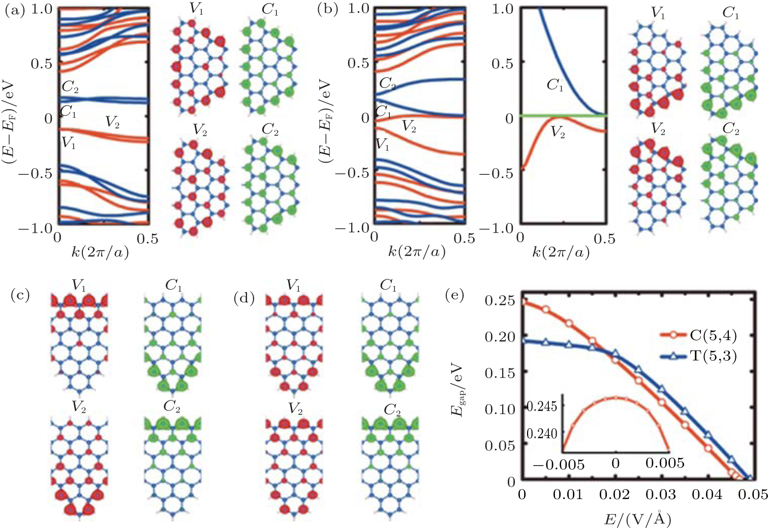
| (a) Band structures and charge distributions of the edge bands V 1, V 2, C 1, and C 2 for C(5,4) without electric field. (b) Same as panel (a) but under E ext = 0.047 V/Å. The right-band structure is the enlargement of the left one. Panels (c) and (d) are the charge distributions of the four edge bands for T(5,3) with electric field E ext = 0 and 0.049 V/Å, respectively. In band structures the black (red) and dark gray (blue) color denote the majority and minority spin states, while in charge distribution pictures the black (red) and gray (green) color label the majority and minority spin charges, respectively. (e) Energy gap of C(5,4) and T(5,3) as a function of E ext. Inset shows the gap of C(5,4) near E ext = 0.[ 68 ] |
 |