†Corresponding author. E-mail: zhoujun@nbu.edu.cn
*Project supported by the National Natural Science Foundation of China (Grant Nos. 61275153 and 61320106014), the Natural Science Foundation of Zhejiang Province, China (Grant No. LY12A04002), the Natural Science Foundation of Ningbo City, China (Grant Nos. 2010D10018 and 2012A610107), and the K. C. Wong Magna Foundation of Ningbo University, China.
According to the plasmon hybridization theory, the plasmon resonance characteristics of the gold nanocrescent/nanoring (NCNR) structure are systematically investigated by the finite element method. It is found that the extinction spectra of NCNR structure exhibit multiple plasmon resonance peaks, which could be attributed to the result of the plasmon couplings between the multipolar plasmon modes of nanocrescent and the dipolar, quadrupolar, hexapolar, octupolar, decapolar plasmon modes of nanoring. By changing the geometric parameters, the intense and separate multiple plasmon resonance peaks are obtained and can be tuned in a wide wavelength range. It is further found that the plasmon coupling induces giant multipole electric field enhancements around the tips of the nanocrescent. The tunable and intense multiple plasmon resonances of NCNR structure may provide effective applications in multiplex biological sensing.
Localized surface plasmon resonance (LSPR) in noble metallic nanostructure, serving as a superior nanoscale optical control approach, plays a crucial role in designing and improving wavelength-tuned optical devices and high sensitive sensors.[1– 4] When the frequency of the incident wave is virtually identical to the collective electron vibrational frequency, the localized surface plasmons of the noble metallic nanostructure can be effectively excited and will engender a strong electromagnetic response to enhance the signals of surface-enhanced Raman scattering (SERS) and the surface-enhanced fluorescence (SEF).[5– 7] As is well known, as the non-destructive and ultrasensitive spectroscopic analysis techniques, SERS and SEF are more suitable to detecting the biological tissues by using the incident radiation in the “ window of optical transparency” , i.e., in the visible and the near infrared (NIR) wavelength region.[8, 9] And, by controlling the geometric and physical parameters of nanostructures such as size, morphology and metal materials, their predominant LSPR bands could be tuned in a wide scope approximately up to incident radiation.[10] Therefore, the plasmon resonance peaks of nanostructures can be located in the “ window of optical transparency” to largely improve the figure of merit (FOM) of biosensor.
In the last few years, much research efforts have been devoted to the design and fabrication of various functional plasmonic nanostructures.[11– 13] These nanostructures have their own optical bands in the absorption or extinction spectra. For instance, the gold or silver spherical nanoparticles have only one plasmon resonance extinction peak.[14] The nanotriangles have a strong peak in their absorption spectrum.[15, 16] The nanorods have two plasmon resonance peaks: a weak transversal mode peak and an intense longitudinal mode peak.[17] The nanoshells also have two plasmon resonance peaks which are defined as the antibonding mode peak at shorter wavelength and the bonding mode peak at longer wavelength resulting from the plasmon hybridization, but the antibonding mode peak is very weak.[18] For nanocubes, there are several plasmon resonance peaks in the extinction spectra while only a strong peak can be well distinguished from them.[19] As we have seen, the most of the existing noble metallic nanostructures have only an intense plasmon resonance band due to their simple geometry. It is a regretful reality that the LSPR characteristics of these nanostructures are impossible to implement multiplex sensing for the applications in biological and chemical fields.
In fact, some researchers have paid their attention to designing and fabricating the complex geometry of nanostructure for obtaining the multiple plasmon resonances. Prodan et al. have found that for a noble metallic compound nanostructure, the plasmon hybridization can form the robust antibonding and the bonding plasmon modes and is used to explain the plasmon resonance properties.[20] Hao et al. have reported that the non-concentric metallic ring/disk nanocavity with symmetry breaking can produce the distinct dipolar, quadrupolar peaks and other high order resonance peaks in the extinction spectra due to the couplings between the multipolar plasmon modes.[21] Zhu et al. have proposed that a multilayer gold shell nanostructure can be used to achieve the multiple plasmon resonances which result in the four intense plasmonic bands in the absorption spectrum.[22] On the other hand, it is possible to gain multiple plasmon resonances by combining the simple geometric nanostructures into a complex one. As a typical example, the disk-ring nanostructure has outstanding advantages of structurally tunable plasmon resonances and easily exciting multipolar Fano features due to the hybridization of the disk’ s dipole mode and the ring’ s higher-order modes.[23] Moreover, the nanocrescent cylinder-nanostrip structure exhibited tunable near-field optical resonance and giant enhancement at the tips of nanocrescent cylinder as the plasmonic hot spots.[24] Accordingly, the plasmon coupling between nanocrescent and nanoring is expected to achieve tunable multiple plasmon resonance bands and intense electric-field enhancement.
In this paper, we numerically study the plasmon resonance properties of gold nanostructure consisting of a nanocrescent and a nanoring by using the two-dimensional finite element method (2DFEM). It is desired to acquire intense multiple plasmon resonance peaks in the extinction spectrum of the proposed gold nanostructure denoted as nanocrescent/nanoring (NCNR) structure. For various geometric parameters such as the gap between nanocrescent and nanoring, NCNR structure demonstrates the multiple plasmon resonance characteristics and its extinction spectrum is intensely dependent on the geometry of NCNR structure. Furthermore, the physical mechanism and tunability of the plasmon peaks are also investigated for the individual nanocrescent and the NCNR structure. And, the local electric field around the tip of the nanocrescent has a strong enhancement by the coherent coupling between the multipolar modes of nanoring and nanocrescent.
The NCNR structure, shown in Fig. 1(a), is a combination of a crescent-shaped gold nanocylinder and a gold nanoring. A large number of such gold nanocrescent cylinders can be fabricated on a glass substrate by nanosphere template lithography with controlled angular deposition of gold, [25] followed by conventional e-beam lithography of the gold nanoring. The NCNR structure is schematically shown in Fig. 1(b) with geometry parameters, in which Rout is the outer radius of nanocrescent, Rin the inner radius of nanocrescent, r the outer radius of nanoring, d the distance between the centers of nanocrescent and nanoring, g the gap width, t the wall thickness of nanoring, and w the distance between two tips of nanocrescent. As shown in the insert in Fig. 1(b), by making a circular cut along the top end of nanocrescent, two half circle tips with radius s are formed. The tip-to-tip distance w changes with tip radius s and center-to-center distance d. Here the linked line
In our research, the extinction cross section of the NCNR structure is derived as the sum of the scattering and absorption cross sections. The scattering cross section of the NCNR structure is calculated by integrating scattered power flux over an enclosed surface outside the NCNR structure, while the absorption cross section is calculated by integrating time-average resistive heating on the NCNR structure.[28, 29] And the extinction cross section spectrum of the NCNR structure is dependent on the geometry parameters to be used to analyze the plasmon resonance characteristics. Moreover, according to Mie theory in the quasistatic approximation, [30] the field enhancement of NCNR structure is closely related to the metallic dielectric constant and the geometry parameters of nanostructure. We will calculate the electric field enhancements at the tip of the nanocrescent in the NCNR structure for discussing the variation of the “ hot spot” .
First, the geometrical parameters of the nanocrescent in the NCNR structure are determined by calculating the extinction cross section of individual gold nanocrescent. The polarization and the wave vector of incident light are the same as ones in Fig. 1(b). As is well known, the extinction spectra and the localized electric field of the nanostructures with sharp corners (edges) are greatly affected by the shapes of sharp corners (edges).[31, 32] Figure 2 shows the extinction spectra of individual nanocrescent with various values of radius s of half circle tips. At s = 0.5 nm, a dipole resonance peak at a wavelength of 994 nm, a quadrupole one at 593 nm and a shoulder peak at 540 nm are found. The shoulder peak arises from the structural discontinuity of the tip of nanocrescent. At s = 1 nm, the extinction spectrum exhibits two distinct peaks, that is, the dipole resonance peak at 897 nm and the quadrupole resonance peak at 559 nm. At s = 3 nm, the intensity of dipole resonance peak at 751 nm is maximum and the quadrupole resonance peak at 522 nm turns to be weak. As s increases from 0.5 nm to 12 nm, all of the dipole peaks are blue-shifted, meanwhile, the quadrupole peaks decline gradually to disappear. It is similar to the LSPR behaviors of nanorod which is excited by incident light polarized along the long axis of nanorod.[33] As demonstrated above, it is an easier way to gain the dipole or quadrupole modes in individual nanocrescent for s of 0.5 nm or 1 nm. Accordingly, the nanocrescent with a tip radius of 0.5 nm or 1 nm could be better to design NCNR structure. However, from a viewpoint of preparation technique, the fabrication of the nanocrescent with a tip radius of 0.5 nm is more difficult than that with a tip radius of 1 nm. Therefore, we single out the nanocrescent with a tip radius of 1 nm to design NCNR structure for further study.
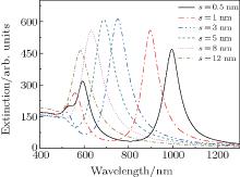 | Fig. 2. Optical extinction spectra of the individual nanocrescent at various values of tip radius and Rout = 60 nm. |
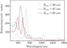
In Fig. 3, we show the extinction spectra of the NCNR structure with different values of Rout for s = 1 nm, t = 2 nm, and g = 2 nm. At Rout = 30 nm, there are one strong, two medium, and a weak plasmon resonance peaks on the extinction spectrum. When Rout increases to 45 nm, the opening of the nanocrescent decreases and the size of nanocrescent increases. The plasmon interaction between nanocrescent and nanoring becomes strong accordingly, which gives rise to four plasmon peaks and a shoulder peak at 645 nm. At Rout = 60 nm, there are five plasmon peaks and a shoulder peak at 765 nm, where only one peak at 668 nm is strong but the others are weaker. In the extinction spectra of the nanostructures, the plasmon resonance peaks may result from the hybridization between plasmon modes of the nanocrescent and nanorings.[34, 35] The analyses of corresponding hybrid plasmon modes provide an effective way to obtain the physical insight into the properties of plasmon resonance peaks and to increase the intensities of multiple plasmon resonances.
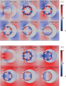
Figure 4(a) shows the distributions of electric field component along the major axis of the NCNR structure, which are calculated at the plasmon resonance peaks of 536, 668, 765, 900, 1147, and 1656 nm in Fig. 3, respectively. For the plasmon resonance wavelength λ = 1656 nm, the surface electric charges of nanoring are separated on two sides of nanoring, and that of nanocrescent on four sides. Meantime, there are singular charge distributions around the tip of the NCNR structure, which may emerge due to the tip effect. As far as we know, like the case of the disk/ring nanostructure, [36] the plasmon resonance peak at 1656 nm can be explained as a result of coherent coupling between the dipolar mode of nanoring, and the quadrupolar mode of nanocrescent (Fig. 4(a, vi)). In the same way, the plasmon resonance peaks at 1147, 900, 765, and 668 nm come from the coherent couplings between the quadrupolar, hexapolar, octupolar, decapolar modes of nanoring, and the quadrupolar mode of nanocrescent, respectively, as shown in Fig. 4(a, vi). Yet the plasmon peak at 536 nm may arise from the coherent coupling of the abnormal multipolar plasmon modes of nanoring and nanocrescent. Figure 4(b) shows the distributions of electric field component perpendicular to the major axis of the NCNR structure at the different plasmon resonance wavelengths. It clearly displays the multipolar plasmon modes induced by surface charges of the nanoring but could not exhibit those of the nanocrescent because the electric field component of the nanocrescent is greatly affected by the incident polarization perpendicular to the major axis of the NCNR structure, which is different from that of Fig. 4(a).
Figure 5 shows the distributions of the electric field intensity of the NCNR structure at the different plasmon resonance wavelengths. Here the structure parameters of NCNR structure and incident light are the same as those of Fig. 4. It can be clearly seen that the enhanced electric fields are located at the tips of the nanocrescent for a plasmon resonance wavelength of 536 nm, and mainly distributed around the tips of the nanocrescent and the gaps between the nanoring and the nanocrescent for the cases of the plasmon resonance wavelengths of 668 nm and 765 nm. While the plasmon resonance wavelengths equal 900, 1147, and 1656 nm, respectively, the enhanced electric fields are present at the gaps between the nanoring and the nanocrescent in NCNR structure.
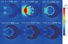 | Fig. 5. Distributions of electric field intensity of the NCNR structure for the plasmon resonance wavelengths of (i) 536, (ii) 668, (iii) 765, (iv) 900, (v) 1147, and (vi) 1656 nm. |
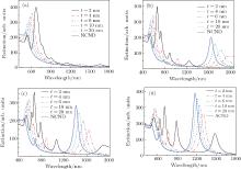
As discussed above, the NCNR structure with Rout = 60 nm is interesting because its extinction spectrum exhibits more plasmon resonance peaks. Subsequently, the influences of the wall thickness t and the gap width g on the plasmon resonances properties of the NCNR structure are analyzed to acquire the intense and separate multiple plasmon resonance peaks. For the NCNR structure with g = 2 nm in Fig. 6(a), with the increase of t value, the number of plasmon resonance peaks gradually decreases and their intensities grow weak. While g = 4 nm and t = 2 nm, there are five intense plasmon peaks and a weak peak at 1940 nm as denoted with the solid line in Fig. 6(b). And, all plasmon resonance peaks are blue-shifted gradually with the increase of t, and then, the plasmon resonance peaks in visible wavelength turn to be one plasmon peak similar to that of the NCND structure. In Figs. 6(c) and 6(d), the right peaks in the infrared range are remarkably blue-shifted and the intensities increase, especially, for t = 20 nm, and the extinction spectrum of the NCNR structure is almost the same as that of the nanocrescent/nanodisk (NCND) structure. It could be explained that the plasmonic peculiarity of nanoring becomes more and more like that of nanodisk with the value of t increasing. Besides, it is clearly observed that the NCNR structure with wall thickness t = 2 nm can obtain more plasmon resonance peaks, and the intense and separate plasmon resonance peaks can be easily received by adjusting the gap width g.
Furthermore, the near-field enhancements of the individual nanocrescent and the NCNR structures dependent on the wavelength are shown in Fig. 7. The solid line represents the electric field enhancement spectrum of the tip of the nanocrescent. The dashed and dotted lines are the electric field enhancement spectra of the tip of the nanocrescent in the NCNR structures. It is apparent that the field enhancement of the NCNR structure with g = 10 nm is higher than those of the individual nanocrescent and the NCNR structure with g = 2 nm for most of plasmon excitation wavelengths, especially at 900 nm. Nevertheless, there are more electric field enhancement peaks in the electric field enhancement spectrum of the NCNR structure with g = 2 nm. It is worth pointing out that, comparing Fig. 7 with Fig. 2 and Fig. 6, the positions of peaks in the electric field enhancement spectrum of the NCNR structure are corresponding to those of the plasmon resonance peaks of the NCNR structure. It illustrates that the greater electric field enhancement can be obtained at the plasmon resonance wavelength. As is well known, the giant electric field enhancement of noble metal nanostructure can enormously improve the SERS and SEF characteristics of analytes bound on the nanostructures to achieve a super-low limit of detection.[37, 38] Obviously, the NCNR structure with t = 2 nm and g = 10 nm is not only to acquire the enormous electric field enhancement, but also to generate more separated plasmon resonances at different wavelengths in the extinction spectrum. And, the plasmon resonance characteristics of the NCNR structures can be tuned by their geometric parameters such as the wall thickness t or the gap width g. Therefore, it is an advantage of the NCNR structure to gain an intense and multipolar plasmon resonance performance.
In this work, we investigate the plasmon resonance characteristics of the individual nanocrescent and the NCNR structure by using the FEM. The numerical analysis demonstrates that the extinction spectra of the NCNR structure are intensively dependent on its geometric parameters. Especially, the number of plasmon resonance peaks of the NCNR structure grows with increasing the outer radius of the nanocrescent. Further, the distributions of electric field induced by surface charges are investigated to analyze the plasmon hybridization in the NCNR structure. And those distributions of electric field components clearly show that the multiple plasmon bands of the NCNR structure come from the coherent couplings between the multipolar plasmon modes of nanocrescent and nanoring such as dipolar, quadrupolar, hexapolar, octupolar, decapolar plasmon modes. Moreover, the intensity and number of the plasmon resonance peaks are effectively regulated by changing the wall thickness and gap width of the NCNR structure. In addition, the phenomenon of the giant enhancement of local electric field at the tips of the NCNR structure is explained as the result of multiple plasmon resonance excitation. As a consequence, the optical properties of the NCNR structures can be used in multiplex biological sensing.
| 1 |
|
| 2 |
|
| 3 |
|
| 4 |
|
| 5 |
|
| 6 |
|
| 7 |
|
| 8 |
|
| 9 |
|
| 10 |
|
| 11 |
|
| 12 |
|
| 13 |
|
| 14 |
|
| 15 |
|
| 16 |
|
| 17 |
|
| 18 |
|
| 19 |
|
| 20 |
|
| 21 |
|
| 22 |
|
| 23 |
|
| 24 |
|
| 25 |
|
| 26 |
|
| 27 |
|
| 28 |
|
| 29 |
|
| 30 |
|
| 31 |
|
| 32 |
|
| 33 |
|
| 34 |
|
| 35 |
|
| 36 |
|
| 37 |
|
| 38 |
|


