
Compact, temperature-stable multi-gigahertz passively modelocked semiconductor disk laser
[Song Yan-Rong†a)  , Guoyu He-Yang
a) , Zhang Pengb) , Tian Jin-Ronga) ]
, Guoyu He-Yang|
|


†Corresponding author. E-mail: yrsong@bjut.edu.cn
*Project supported by the National Natural Science Foundation of China (Grant No. 61177047) and the Key Project of the National Natural Science Foundation of China (Grant No. 61235010).
We present a compact passively mode-locked semiconductor disk laser at 1045 nm. The gain chip without any post processing consists of 16 compressively strained InGaAs symmetrical step quantum wells in the active region. 3-GHz repetition rate, 4.9-ps pulse duration, and 30-mW average output power are obtained with 1.4 W of 808-nm incident pump power. The temperature stability of the laser is demonstrated to have an ideal shift rate of 0.035 nm/K of the lasing wavelength.
Multi-gigahertz picosecond pulse trains are suitable for a wide variety of applications, such as optical clocking, [1] frequency conversion, [2] high-speed electro– optic sampling, [3] time-resolved spectroscopy, [4] and the primary light source for telecommunication systems.[5] For a long time, mode-locked solid-state lasers and edge-emitting semiconductor lasers have been the dominators in the field of multi-gigahertz picosecond pulse resources. In recent years, passively mode-locked semiconductor disk lasers (SDLs, also known as optically pumped vertical-external-cavity surface-emitting lasers), have been demonstrated to be capable of generating multi-gigahertz pulses with high average output power and good beam quality.[6– 9] By comparison, SDLs are cost-effective hence attractive for their potential substitutes for mode-locked solid-state lasers or edge-emitting semiconductor lasers in some applications.[10– 12]
For mode-locked edge-emitting semiconductor lasers, it is difficult to produce high output power and maintain single transverse mode operation simultaneously because of the limitation of the usable mode area, and the optical damage. They need complex configurations such as tapered amplifier section[13] or master-oscillator-power-amplifier system[14] to increase the output power. In contrast, the output power of mode-locked SDL can be scaled conveniently through extending the pump area under intensive pump, since the surface-emitting geometries allow much larger mode areas (particularly when optical pumping is used, the spatially homogeneous excitation can be easily achieved). Along with a properly designed fundamental mode external cavity, single transverse mode operation can be supported at the same time.[15, 16]
Compared with the mode-locked solid-state laser, SDL possesses the advantage of a large gain cross-section which suppresses Q-switching instability.[17] SDL therefore is ideally suited for multi-gigahertz repetition-rate mode-locking in combination with high average output power. The SDL has other advantages, e.g., more than 30-nm gain bandwidth of the quantum wells (QWs) is sufficient to support sub-picosecond pulses, and the interband transition absorption of pump power in the barriers of QWs offers great freedom in the selection of pumping wavelength. In addition, the well-developed bandgap engineering allows SDL with flexible wavelength coverage from visible to mid-infrared; [18, 19] and the state-of-the-art semiconductor processing supports lateral integration of passively mode-locked SDL based on novel low saturation fluence quantum dot semiconductor saturable absorb mirror (SESAM).[20]
Since the first report of a passively mode-locked SDL, [6] performance of the mode-locked SDL has been improved significantly: pulse duration increased up to 60 fs at 1-GHz repetition rate and 35-mW output power; [21] repetition rate has increased up to 50 GHz with 3.3-ps pulse duration and 100-mW output power by a low saturation fluence quantum dot SESAM; [22] average output power has increased up to 5.1 W at 1.71-GHz repetition rate and 682-fs pulse duration by a quantum-well SESAM; [23] a tunable repetition has been enhanced from 6.5 GHz to 11.3 GHz by a quantum dot (QD) SESAM; [24] a record low pulse repetition rate of 99.6 MHz with an average output power of 30 mW and pulse duration of 20 ps[25] and an all quantum dot mode-locked semiconductor disk laser emitting at 655 nm have been obtained.[26] However, the lasing wavelength of an SDL (GaAs based) has a red shift at a rate of about 0.3 nm/K with increasing temperature because of the intrinsic characteristic of the QWs, [15, 27] and this problem has not been solved so far. In this paper, we demonstrate a picosecond passively mode-locked SDL at multi-gigahertz repetition rate. The gain chip is not treated by any post processing (such as substrate-removing and heatspreader-bonding). The fabrication is quite simple and the configuration is compact. Although some other saturable absorbers such as carbon nanotubes and graphene have been widely used in mode-locked lasers, [28– 32] SESAM is still a major saturable absorber which is used in SDL. The gain chip of the SDL and the SESAM are both semiconductor materials, which are easy to obtain mode-locked pulse trains by SESAM, so in our experiment, we still use SESAM as a saturable absorber. Temperature stability of the laser is achieved using the symmetrical step QWs in the active region, which will be discussed below.
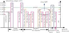
Figure 1 shows the epitaxial structure of the semiconductor wafer and the absorbing edges of the corresponding materials. The metal-organic chemical vapor deposition (MOCVD) grown wafer includes the following parts: a substrate, a distributed Bragg reflector (DBR), multiple quantum wells (MQWs), a window layer, and a cap layer. The DBR works as one of the reflectors in the laser; the MQWs are the active region; the window layer is used to prevent the carriers against the nonradiative combination at the surface; and the cap layer is added to protect the epitaxial structure from being oxidized. In our wafer design, the DBR contains 30 pairs of alternating GaAs and AlAs layers; the active region consists of 16 non-compensated compressively strained In0.2Ga0.8As QWs which are sandwiched by the Al0.05Ga0.95As barriers and located at the antinodes of the standing wave of the laser in the micro-cavity to form the well-known periodic resonant gain (PRG) structure.[33] The Al0.05Ga0.95As barriers, also as pump absorbers, are designed in such a way that they can provide barriers as high as possible to confine the carriers while their absorbing edges should be below the pump wavelength in order to absorb the pump efficiently. Between the well and the barrier there is a GaAs spacer layer, which is helpful to improve the quality of wafer growth and has been proven to enhance the capture of carriers into the well.[34] The Al0.05Ga0.95As barrier, the GaAs spacer, along with the In0.2Ga0.8As well together form a so-called symmetrical step QW (Fig. 1). A transparent Al0.6Ga0.4As layer at both lasing and pumping wavelengths provides a high barrier as the window layer. A GaAs cap layer is used to finish the growth.
 | Fig. 1. Epitaxial structure of the gain chip and the absorption edges of the corresponding materials. |
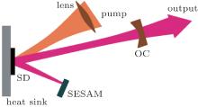
 | Fig. 2. Cavity setup used for the passively mode-locked SDL. |
The V-shaped cavity setup used for the passively mode-locked SDL is shown in Fig. 2. A 2 mm× 2 mm unprocessed gain chip cleaved off the wafer is directly mounted on a copper heat sink and is temperature-controlled by a Peltier cooler. The semiconductor chip with lower temperature provides higher output power and higher slope efficiency which had been demonstrated before, [35] so heat sink temperature is set to be 3 ° C in this work. The back plate of the entire device is water-cooled. A fiber-coupled 808-nm pump radiation is collimated and focused on the semiconductor disk at an angle of about 45, and the diameter of the pump spot is approximately 100 μ m. The gain chip is used as a folding mirror, and the laser cavity is ended by a low-temperature grown SESAM and a highly reflective plane-concave output coupler (OC). The folded angle of the cavity is smaller than 10° to reduce the astigmatism.
The curved OC determines a small mode area on the SESAM, such that the saturation energy of the absorber is lower than the saturation energy of the gain medium as required for pulse formation.[36] In the experiment, the total cavity length is approximately the same as the radius of curvature of the OC to force the laser to operate at the edge of the stable region. The lengths of OC arm and SESAM arm are about nine tenths and one tenth of the total cavity length, respectively, to produce a laser spot about 100 μ m on the gain chip for matching the pump spot. The ratio of the area between the spot on the gain chip and that on the SESAM is about 25. With a fixed optimum laser spot on the gain chip, we adjust the lengths of the SESAM arm and the OC arm to obtain a stable continuous-wave (CW) mode-locking operation.
We use an Infiniium54833A oscilloscope (Agilent Technologies) to monitor the mode-locked pulse trains. The output beam is sent to an FR-103XL autocorrelator (Femtochrome Research) to obtain the autocorrelation trace. Meanwhile, a fast 818-BB-35FInGaAs PIN photoelectric detector (Newport) with a 10-GHz bandwidth and < 35-ps rise time and a 40-GHz E4447A spectrum analyzer (Agilent Technologies) are used to receive the optical pulses and obtain the radio-frequency (RF) spectrum.
Firstly, a plane-concave mirror with a radius of curvature of 100 mm is used as the OC. The measured and sech2 fitted autocorrelation trace of the mode-locked pulse trains are shown in Fig. 3(a). The sech2 fit indicates that the ideal width (full width at half maximum (FWHM)) of the pulses is 5.0 ps, which is about 4.2 times the Fourier transform limited sech2 pulse duration of 1.2 ps, according to the inserted optical spectrum with 0.96 nm in width. It is known that for a passively mode-locked SDL, the presence of chirp in the pulses is inevitable because of the saturation effect (also known as phase modulation effect) of the gain medium and the SESAM. With some dispersion-controlled elements such as an etalon, the above phase modulation effect can be counteracted and the transform-limited pulse trains can be produced.[7]
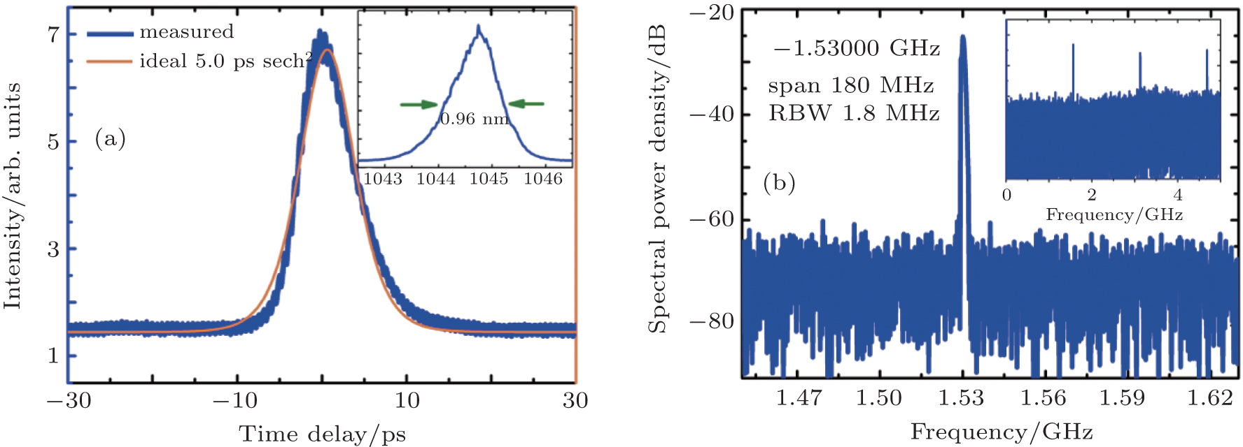 | Fig. 3. Measured and sech2 fitted autocorrelation trace (a) and RF spectrum (b) of the mode-locked pulses. The inset in panel (a) shows the optical spectrum and the inset in panel (b) shows the RF spectrum on a 5-GHz span. The radius of curvature of the OC is 100 mm. |
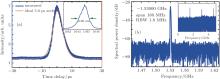
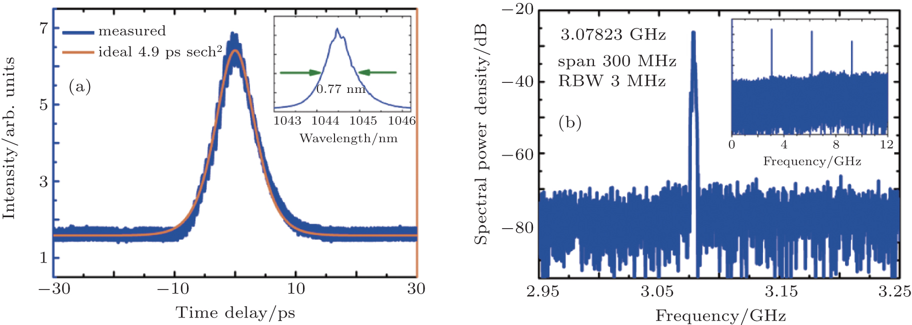 | Fig. 4. Measured and sech2 fitted autocorrelation trace (a) and RF spectrum (b) of the mode-locked pulses. The inset in panel (a) shows the optical spectrum and the inset in panel (b) shows the RF spectrum on a 12-GHz span. The radius of curvature of the OC is 50 mm. |
Figure 3(b) shows the RF spectrum of the laser. The frequency span is 180 MHz and the resolution bandwidth (RBW) is 1.8 MHz. The inset shows the frequency spectrum on a 5-GHz span. As shown in Fig. 3(b), the fundamental frequency is 1.5 GHz, corresponding to a round-trip repetition rate of 100-mm cavity. The RF spectrum trace is free from sidebands down to a level of − 35 dB, demonstrating that the SDL exhibits stable CW mode-locking with no Q-switching instability.
When the OC with 100-mm curvature radius is replaced by the OC with a 50-mm curvature radius, the autocorrelation trace and the RF spectrum of the mode-locked laser are shown in Figs. 4(a) and 4(b). It can be seen from Fig. 4(a) that the sech2 fitted pulse duration is 4.9 ps, which is about 2.3 times the Fourier transform-limited sech2 pulse width of 2.1 ps, according to the inserted 0.77-nm-wide optical spectrum. Figure 4(b) shows a 3-GHz RF of the mode-locked pulses, and this is consistent with the round-trip repetition rate of 50-mm cavity. The RF spectrum trace is free from sidebands down to the level of − 45 dB, again demonstrating no Q-switching instability in the CW mode-locked SDL.
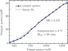
Figure 5 shows the average output power versus pump power under 3-° C heat sink temperature. The repetition is 3 GHz, and the laser operates in a circular TEM00 mode. A maximum average output power of 30 mW is reached with 1.4-W pump power; the slope efficiency (SE) and the optical-to-optical conversion efficiency are about 3.1% and 2%, respectively. Limitations of the output power and SE mainly result from the thermal problem. With the increasing of temperature, the gain of the QWs will decrease sharply, the redshift of the laser wavelength will detune the PRG structure, and nonradiative recombination will become dominant.[37] All of the above factors are compounded until finally the thermal rollover of the laser occurs and the device stops lasing.
The two kinds of technologies introduced in the thermal management of SDLs are substrate-removal[7, 15, 16, 23] and the use of heatspreader.[38] In the former method, the wafer should be grown following a reverted sequence (i.e., firstly an etch-stop layer on the substrate, then the cap layer, the window layer, the QWs, and finally the DBR). Then the chip is soldered on the DBR-side down on the heat sink and the substrate can be removed by chemical etching. As to the latter process, materials with high thermal conductivity (e.g. diamond, SiC or sapphire) and good transparency for designed laser wavelength are selected as the heatspreader, and are bonded to the gain chip on the active region side using liquid capillary bonding technique. By employing the above thermal management, the heat dissipation from the active region can be improved effectively, the rollover of the laser can be retarded and the output power can be enhanced significantly.
 | Fig. 5. Average output power of the mode-locked laser at 3-GHz repetition rate versus pump power at a temperature of 3 ° C and its linear fitting. |
Generally, a QW SDL suffers strong temperature sensitivity of the gain medium (e.g., for a GaAs-based SDL, the lasing wavelength is red-shifted at a typical rate of about 0.3 nm/K with rising temperature). The intrinsic temperature dependence of the QW gain arises from three effects: the shift of the semiconductor band gap, the thermally excited escape of the carriers, and the variation of the Fermi factor.[39] In our wafer design, we use the so-called symmetrical step QW in the active region to partly overcome the above temperature sensitivity. Compared with a general QW, a step QW at least has two characteristics. The first is its closer distribution of the energy levels near the ground level of the conduction band, which is favorable to the producing of a broad and flat gain. The second is its more effective confinement thus less escape of thermally excited carriers and this is also contribution to the broad and flat gain. The broad and flat gain spectrum of step QWs offers the advantage of a temperature-independent matching of the gain maximum with a given cavity resonance, and this can be expected to result in temperature-independent device operation.
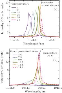
Figures 6(a) and 6(b) show the laser spectra under different heat sink temperatures and different pump powers. The average redshift rate of the lasing wavelength in Fig. 6(a) is about 0.035 nm/K, which is far smaller than 0.3 nm/K, the value of the general QW SDL. It can be concluded from Fig. 6(a) that the shifting rate becomes smaller at higher temperature. Since the increased pump power will also cause temperature to rise, we measure the lasing wavelengths under different pump powers and the results are shown in Fig. 6(b). As can be seen from Fig. 6(b), the average shift rate of the wavelength is about 6× 10− 5 nm/kW· cm− 2. Like Fig. 6(a), the shifting rate becomes smaller at higher pumping powers.
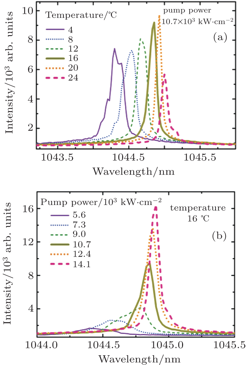 | Fig. 6. Laser spectra under different heat sink temperatures (a) and different pump powers (b). |
 | Fig. 7. Dependences of the laser wavelength on temperature and pump power. |
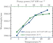
The dependences of lasing wavelength on heat sink temperature and pump power are shown in Fig. 7. From the slow rising parts at the end of the curves in Fig. 7, the tendency that the shift rate of the lasing wavelength becomes smaller at higher temperature or intensive pumping can be seen more clearly.
In this work, we demonstrate a compact passively mode-locked SDL. The CW mode-locking operation at 3-GHz repetition rate, 4.9-ps pulse duration, and 30-mW average output power is obtained by using a low-temperature grown SESAM. Due to the broad and flat gain of the symmetrical step QWs in the active region, the laser shows the ideal temperature stability with a redshift rate of 0.035 nm/K of the lasing wavelength, which is, to our knowledge, the smallest shift rate of a QW SDL so far. The laser can be used as a gigahertz picosecond pulse source in many applications.
| 1 |
|
| 2 |
|
| 3 |
|
| 4 |
|
| 5 |
|
| 6 |
|
| 7 |
|
| 8 |
|
| 9 |
|
| 10 |
|
| 11 |
|
| 12 |
|
| 13 |
|
| 14 |
|
| 15 |
|
| 16 |
|
| 17 |
|
| 18 |
|
| 19 |
|
| 20 |
|
| 21 |
|
| 22 |
|
| 23 |
|
| 24 |
|
| 25 |
|
| 26 |
|
| 27 |
|
| 28 |
|
| 29 |
|
| 30 |
|
| 31 |
|
| 32 |
|
| 33 |
|
| 34 |
|
| 35 |
|
| 36 |
|
| 37 |
|
| 38 |
|
| 39 |
|