†Corresponding author. E-mail: bxiong@tsinghua.edu.cn
‡Corresponding author. E-mail: luoy@tsinghua.edu.cn
*Project supported by the National Basic Research Program of China (Grant Nos. 2012CB315605 and 2014CB340002), the National Natural Science Foundation of China (Grant Nos. 61176015, 61176059, 61210014, 61321004, and 61307024), and the Open Fund of State Key Laboratory on Integrated Optoelectronics, China (Grant Nos. IOSKL2012KF08 and IOSKL2014KF09).
A backside illuminated mesa-structure InGaAs/InP modified uni-traveling-carrier photodiode (MUTC-PD) with wide bandwidth and high saturation power is fabricated and investigated. The device structure is optimized to reduce the capacitance and resistance. For the 22-μm-diameter device, the maximum responsivity at 1.55 μm is 0.5 A/W, and the 3-dB cutoff frequency reaches up to 28 GHz. The output photocurrent at the 1-dB compression point is measured to be 54 mA at 25 GHz, with a corresponding output radio frequency (RF) power of up to 15.5 dBm. The saturation characteristics of the MUTC-PD are also verified by the electric field simulation, and electric field collapse is found to be the cause of the saturation phenomenon.
Analog optical links are attractive for many microwave applications, such as phased array antennas, radio-over-fiber systems, and photonic analog-to-digital conversion, due to their low loss, wide bandwidth, and immunity to electromagnetic interference.[1] In order to improve the performances of the analog links, one of the crucial techniques is to adopt photodiodes (PDs) with a wide bandwidth and high saturation characteristics. The uni-traveling carrier (UTC) structure[2] has been proposed to improve the bandwidth and saturation characteristics of PDs. Compared with the conventional pin PDs, [3] the UTC structure is composed of a heavily doped p-region and an undoped depletion region, in which the holes are collected by the p-electrode with a short relaxation time and only the electrons drift in the depletion region, thus greatly enhancing the bandwidth and output RF power due to the higher velocity of electrons relative to that of holes.[4] The modified uni-traveling carrier photodiode (MUTC-PD) is developed by inserting an undoped InGaAs layer between the heavily doped absorption region and the depletion region of the UTC structure to increase the responsivity and bandwidth, [5] and it is also an important candidate to achieve a wide bandwidth and high saturation performance simultaneously.
The bandwidth of mesa-structure PDs is limited by two primary factors: the resistance– capacitance (RC) time constant and the carrier transport time. In order to obtain PDs with an ultra-high bandwidth, downscaling the mesa area and the absorption region thickness is an effective method.[6] A thinner absorption region leads to a shorter electron transit time and a higher saturation photocurrent, but a smaller mesa area will result in a larger series resistance and a higher current density, seriously limiting the saturation performance of the PD.
Furthermore, due to the decrease of the electric field in the depletion region under a high photocurrent, which is mainly caused by the voltage drop on the series resistance, load voltage swing, and the space-charge effect, the output RF power and bandwidth of PD will seriously degrade.[7, 8] Fortunately, the electron drift velocity can be modulated by optimizing the electric field within the depletion region, thus relieving the carrier accumulation and increasing the bandwidth.[9] Therefore, the analysis of the electric field distribution within the device is crucial for the PD with a small area to achieve a high output RF power.
In our previous work, an output photocurrent as high as 100 mA at 9 GHz was demonstrated in a 40-μ m-diameter device.[10] In this work, the thickness of the absorption layer is decreased to reduce the electron transit time, and the device structure is optimized to reduce the series resistance and capacitance of the MUTC-PD. For a 22-μ m-diameter device, 3-dB bandwidth of 28 GHz is achieved, and the 1-dB compression point of the output photocurrent at 25 GHz is measured to be 54 mA, corresponding to an output RF power of up to 15.4 dBm. The maximum responsivity at 1.55 μ m is 0.5 A/W. Meanwhile, the saturation characteristics of the MUTC-PD under high injection levels are investigated. The electric field distributions within the device under different photocurrents are simulated, which takes the load voltage swing effect and the charge screening effect into consideration. According to the simulated electric field distribution within the depletion region, the saturation of the device is caused by partial field collapse at high photocurrent levels.
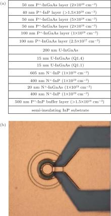
The epitaxial structure as shown in Fig. 1(a) is grown on a semi-insulating InP substrate by metal organic chemical vapor deposition (MOVCD). The absorption region consists of a 300-nm graded doped InGaAs absorption layer and a 200-nm undoped InGaAs layer, the doping concentration decreases from 5× 1018 cm− 3 to 2.5× 1017 cm− 3, which generates a stepped potential profile in the conduction band and helps electrons transit to the depletion region. The depletion region consists of a 200-nm undoped InGaAs layer, a 30-nm InGaAsP transition layer, and a 605-nm InP intrinsic layer. The intrinsic layer is lightly Si-doped to provide a fixed positive ion charge distribution, which will compensate the space-charge effect when the photogenerated electrons diffuse into the depletion region. The charge compensation will effectively adjust the field distribution under high injection levels and improve the saturation performance of the device.[5] The diffusion-block layer is a 400-nm-thick p-doped InP layer.
Similar to the fabrication process described in Ref. [9], backside-illuminated mesa-structure PDs with 22-μ m diameter are fabricated. Two inductively coupled plasma (ICP) dry-etching processes are adopted to define the double mesa structure. The Ti/Pt/Au p-electrode and Ni/Au n-electrode are obtained by magnetron sputtering and lift-off processes. An 800-nm-thick SiO2 layer and a 200-nm-thick SiNx layer are deposited with plasma enhanced chemical vapor deposition (PECVD) to diminish the parasitic capacitance and leakage current. A coplanar waveguide electrode is fabricated on top of the dielectric layers, followed by an up electroplating of 1.5-μ m-thick Au. Finally, a 215-nm-thick SiNx antireflection layer is deposited on the backside of the epitaxial wafer to increase the coupling efficiency. The top view of the device is shown in Fig. 1(b). The shape and the positon of the n-electrode are optimized to achieve low series-resistance and transmission loss.
In order to improve the bandwidth of the MUTC-PD, the device structure is optimized to reduce the capacitance and series resistance. As shown in Fig. 2, compared with our previous device, [9] the diameter of the mesa shrinks from 40 μ m to 22 μ m, while the distance between the mesa edge and the n-electrode is reduced from 10 μ m to 5 μ m. The junction capacitance of the 22-μ m-diameter device is about 30% of that of the 40-μ m-diameter one. In addition, the material volume resistance is reduced to be lower than 2 Ω due to the smaller distance between the mesa edge and the n-electrode.
Figure 3 shows the I– V characteristics of the MUTC-PD before and after optimization. The series resistance is reduced from 10 Ω to 4 Ω by optimizing the device structure and the rapid thermal annealing process. The capacitance of the 40-μ m-diameter device extracted from the measured S11 parameter is about 300 fF, corresponding to an RC time constant limited bandwidth about 8.8 GHz.[9] After optimization, the junction capacitance is reduced to 95 fF, and the calculated RC time constant limited bandwidth of the 22-μ m-diameter device is about 31 GHz, which is about 3.5 times that of the device before optimization.
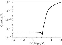
Under 3 V reverse bias, the dark current is smaller than 20 nA, as shown in Fig. 4. The dark current comes mainly from the sidewall leakage current for cylinder-mesa devices.[10] Small dark current is essential for the device to achieve high power performance under high reverse bias. A smooth etched surface is realized by adjusting the etching parameters and the proportion of Ar/Cl2/CH4 gas mixture, [11] and appropriate passivation is also performed by depositing a silicon dioxide layer to reduce the leakage current.
The frequency response of the device is measured using the optical heterodyne method, in which the 100% modulated RF light signal is generated by two lasers.[12] The measured frequency responses at different photocurrent levels under 4 V reverse bias are plotted in Fig. 5. The 3-dB bandwidth of the device is measured to be 28 GHz at a photocurrent of 40 mA. As discussed above, the frequency response of the device is principally RC-limited.
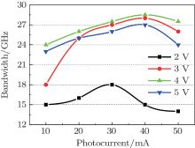
Figure 6 shows the measured bandwidth versus photocurrent under different reverse biases. For the 2 V reverse bias, the depletion region of the device is not completely depleted, so the bandwidth is relatively low. When the reverse bias is increased to 3 V and 4 V, an obvious improvement of the bandwidth performance is observed. Increasing the reverse bias to 5 V, the bandwidth reveals a slight decrease, because now the electric field is out of the range for overshoot velocity.[12] Another obvious feature is the bandwidth enhancement along with the increase of photocurrent before saturation sets in. The bandwidth increases from 18 GHz at 10 mA up to 28 GHz at 40 mA under 3V reverse bias. This dynamic improvement comes from two contributions:[13] 1) as the photocurrent increases, the electric field in part of the depletion region is reduced to around the critical electric values, which allows the electrons to drift at overshoot velocity; 2) the electron transport time is reduced due to the self-induced field in the highly doped absorption region. When the photocurrent is further increased, the bandwidth begins to reduce because of electric field collapse in part of the depletion region at the high photocurrent level.
The output RF power of the device at 25 GHz under 2 V, 3 V, and 4 V reverse biases is shown in Fig. 7. The measured output RF power is about 3-dB lower than the ideal value due to that the measured frequency point is around the 3 dB roll over frequency. Because the bandwidth increases with increasing photocurrent as shown Fig. 6, the output RF power gets closer to the ideal line at high photocurrent. The saturation photocurrent at the 1-dB compression point under 2 V, 3 V, and 4 V reverse biases is 35 mA, 48 mA, and 54 mA, corresponding to the output RF power of 12.1 dBm, 14.8 dBm, and 15.5 dBm, respectively. A higher saturation photocurrent can be expected by adopting the flip-chip bonding technique.[14] The saturation characteristics under different revers biases coincide with the calculated electric fields shown in Fig. 8.
 | Fig. 7. Output RF power of the device under reverse biases of 2 V, 3 V, and 4 V at a frequency of 25 GHz. |
 | Fig. 8. Electric field distributions under (a) 3 V and (b) 4 V reverse biases with different output photocurrents. |
The electric field distributions under 3 V and 4 V reverse biases are shown in Figs. 8(a) and 8(b), respectively. The electric field in the InGaAs depletion region decreases along with the increase of the photocurrent, and begins to collapse when the photocurrent is larger than 40 mA under 3 V reverse bias, while the collapse of the electric field happens for photocurrent larger than 50 mA under 4 V reverse bias. The electric field profiles under different reverse biases are consistent with the above-mentioned bandwidth and output RF power performance. The electric field within the device can be simulated by the photocurrent-Poisson equation, which takes into account the space charge effect, voltage drop and swing under high power illumination. A part of the reverse bias voltage is lost at the high photocurrent level due to the voltage drop on the series resistance and the voltage swinging arising from the alternating photocurrent delivered to the 50-Ω matched load resistance. In addition, the space charge effect is serious under high optical injection levels, especially at the heterojunction interface. This will drastically suppress the electric field and lead to the saturation of the MUTC-PD.
The saturation characteristic of the device is limited by the lowest electric field during the alternating photocurrent period. Saturation occurs when the electric field is screened by the photo-generated electrons in the depletion region, which is thoroughly investigated in our previous work.[8] Charge accumulation at the heterojunction interface will cause saturation to occur at lower photocurrent. By taking the thermal effect and the velocity overshoot effect into consideration, the accuracy to predict the saturation photocurrent can be further elevated.
A wide bandwidth backside illuminated MUTC-PD is achieved by optimizing the device structure, and its saturation performance is investigated. The device exhibits a series-resistance of 4 Ω and a dark current of 20 nA under − 3 V. The 3-dB cut-off frequency is as high as 28 GHz. The output photocurrent at the 1-dB compression point reaches up to 54 mA at 25 GHz, with a corresponding output RF power of 15.5 dBm. The electric field distributions under high photocurrent levels within the device are also simulated, and the results reveal the reason for the saturation phenomenon and the variation of the bandwidth. It is believed that the performance of MUTC-PD can be further improved by optimizing the device structure and the electric field distribution within the depletion region.
| 1 |
|
| 2 |
|
| 3 |
|
| 4 |
|
| 5 |
|
| 6 |
|
| 7 |
|
| 8 |
|
| 9 |
|
| 10 |
|
| 11 |
|
| 12 |
|
| 13 |
|
| 14 |
|


