†Corresponding author. E-mail: jlyu@semi.ac.cn
‡Corresponding author. E-mail: sycheng@fzu.du.cn
*Project supported by the National Natural Science Foundation of China (Grant Nos. 61076063, 61340051, and 61306120) and the Natural Science Foundation of Fujian Province, China (Grant No. 2014J05073).
Ag- and Sn-doped In2S3 thin films were deposited on glass substrates using the thermal evaporation technique. The doping was realized by thermal diffusion. The influences of Ag and Sn impurities on the electrical, structural, morphological, and optical properties of the In2S3 films were investigated. In all deposited samples, the x-ray diffraction spectra revealed the formation of cubic In2S3 phase. A significant increase in the crystallite size was observed after Ag doping, while the doping of Sn slightly decreased the crystallite size. The x-ray photoelectron spectroscopy verified the diffusion of Ag and Sn into the In2S3 films after annealing. The optical study illustrated that Ag doping resulted in a reduction of the optical band gap while Sn doping led to a widening of the gap. Optical properties were investigated to determine the optical constants. Besides, it was found that the resistivity decreases significantly either after Ag or Sn incorporation. The study demonstrates that the Sn-doped In2S3 thin films are more suitable for buffer layer application in solar cells than the Ag-doped In2S3 thin films.
As an n-type semiconductor, indium sulfide (In2S3) thin films have attracted much attention nowadays due to their potential applications in photovoltaic devices.[1– 3] For many technological applications, In2S3 is an important material because of its photoconductive behavior, wide band gap, and stability.[4] Since In2S3 is nontoxic and has a wider band gap than CdS, which can improve the light transmission in the blue wavelength region, it can be used as an effective substitute for CdS in CIGS based solar cells. CIGS based solar cells using In2S3 as the buffer layer could reach an efficiency of 16.4%, which is close to that achieved using CdS as the buffer layer.[5] In2S3 shows three different crystallographic phases, i.e., α , β , and γ .[6] At room temperature, β -In2S3 is the most stable phase, which has high concentrations of crystallizes, octahedral and tetrahedral vacancy sites in a defect spinel lattice.[7]
Impurity doping is an effective approach to improve the physical properties of the In2S3 thin films. However, there are only a few works investigating the doping of In2S3 films. Kamoun et al. reported that an increase in adsorption of oxygen could be observed in the samples with Al doping.[8] Barreau et al. found that doping In2S3 with Na could lead to a better conductivity and a wider band gap.[9] Becker et al. found that Sn doping led to low resistivities of samples.[10] Mathew et al. found that the incorporation of Ag could result in enhanced photosensitivity, conductivity, and crystallinity in the films.[11] In this paper, the Ag and Sn doped In2S3 thin films are prepared by thermal evaporation technique. We analyze the dopant mechanism and investigate the influence of Ag and Sn doping on the electrical, optical, and structural properties of the In2S3 thin film.
Glasses were used as the substrates in the experiment. Before deposition, we cleaned the glasses with deionized water, acetone, and ethanol using an ultrasonic cleaner for 15 min respectively. Sn and Ag-doped In2S3 thin films were deposited on the glass substrates using the thermal evaporation method (DMDE-450 deposition equipment). The Ag patch with 99.9% purity, Sn powder (99.99%), and In2S3 powder (99.98%) were used as the source materials. The distance between the source materials and the substrates was kept constant 11.5 cm. During evaporation, the pressure of the chamber was about 2 × 10− 3 Pa. The doped films can be obtained by doping a thin layer of Ag or Sn on the In2S3 layer using the thermal evaporation technique. The doping concentrations of Ag and Sn were both set at 4 at.%, which was estimated by the weight of the In2S3 source material. The Ag/In2S3, Sn/In2S3 bilayer and undoped In2S3 samples were annealed in Ar atmosphere at 300 ° C for 1.5 h for the diffusion of the metals.
The structure of the prepared films was characterized by the x-ray diffraction (XRD) in the range of 10° – 80° with Cu Kα radiation source (λ = 1.5406 Å ). The optical reflectance and transmittance spectra were measured in the range from 350 nm to 1200 nm with a Cary 5000-scan UV– vis– NIR spectrometer. The optical constants such as the extinction coefficient and the refractive index were also obtained from the reflectance and transmittance spectra. Compositional analysis was carried out with x-ray photoelectron spectroscopy (XPS). The surface morphologies were investigated by atomic force microscopy (AFM) and scanning electron microscopy (SEM). An HMS-3000 Hall measurement system was used to study the electrical properties such as the carrier concentration and the resistivity of the films.
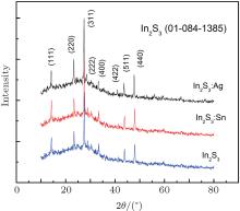
The x-ray diffraction patterns of the prepared films are shown in Fig. 1. We can see that all samples are polycrystalline and all the diffraction peaks can be attributed to the cubic In2S3 phase (PDF 01-084-1385). No new phases are observed either after Ag or Sn doping, which means that there is no new crystalline formed and no change in the structure of In2S3 due to the incorporation of Ag or Sn. This phenomenon is in accordance with that reported in the previous works.[11, 12]
The average crystallite size (D) can be estimated from the strongest diffraction peak (311) using Scherrer’ s equation[13]

where k is a constant, θ is the Bragg angle, λ is the wavelength of the Cu Kα radiation line, and β is the full width at half maximum corresponding to the preferred orientation (311). The calculated crystallite sizes are summarized in Table 1. Since the ionic radius of In3+ is 0.81 Å , which is much smaller than that of Ag+ (1.26 Å ), a considerable increase in the crystallite size can be observed after Ag doping, as shown in Table 1. After Sn doping, there is a slightly decrease in the crystallite size, which may be due to the smaller ionic radius of Sn4+ (0.71 Å ) compared to that of In3+ (0.81 Å ).[14]
| Table 1. Grain sizes of doped and undoped samples. |
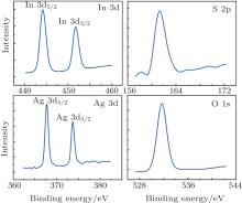
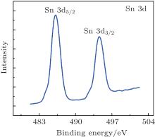
The XPS can evaluate the elemental compositions of the films and the bonding states for each constituent element. All the XPS spectra are calibrated by the C 1s peak (284.6 eV). The XPS spectra of the Ag-doped In2S3 film are shown in Fig. 2, which proves the diffusion of Ag into the In2S3 film after annealing. Binding energies that correspond to the elemental form of Ag+ (373.9 eV for Ag 3d3/2, 367.8 eV for Ag 3d 5/2) can be observed. The binding energies of In and S (452.4 eV and 444.8 eV for In 3d3/2 and In 3d5/2, respectively, 161.9 eV for S 2p) indicate the formation of In2S3.[15] The binding energy of oxygen (532.2 eV) corresponds to surface contaminant.[16] For the Sn-doped In2S3 film, the Sn 3d photoelectron peaks are shown in Fig. 3, which verifies the diffusion of Sn into the In2S3 film. The peak at 486.8 eV for Sn 3d5/2 corresponds to the Sn4+ state and the binding energy of 495.2 eV corresponds to Sn 3d3/2.[17]
The plane view AFM images of the doped and the undoped In2S3 films are shown in Fig. 4. The surface of the undoped film is composed of spherical particles uniformly distributed over all the scanned area. These spherical particles become bigger after the Ag incorporation, and the particle is of a large size exceeding 60 nm, which is much larger than the grain size (42.13 nm) calculated from the XRD result. It might be that the grain has undergone a significant growth to incorporate the nearby grains during the annealing process. The surface of the Ag-doped film is not smooth enough and the height difference can reach about 60 nm. The unsmooth surface obviously results from the large particles that are produced in the In2S3 layer. For the Sn-doped film, plenty of little particles are uniformly dispersed in the layer without obvious cracks.
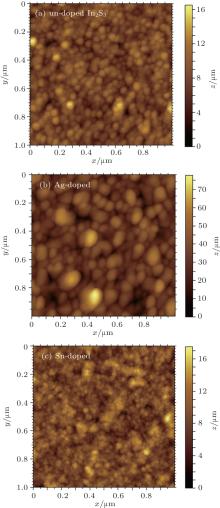 | Fig. 4. AFM images (1 μ m× 1 μ m) of (a) the un-doped, (b) the Ag-doped, and (c) the Sn-doped films. |
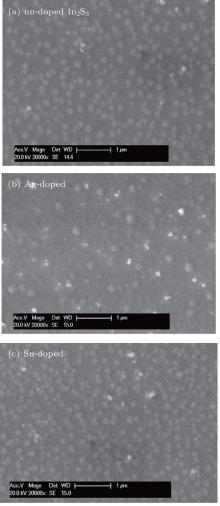
The SEM micrographs of the films are shown in Fig. 5. It is obvious that the crystallite size is increased after Ag doping and decreased after Sn incorporation, which supports the results obtained from the XRD analysis.
The transmission spectra of In2S3, In2S3:Sn, and In2S3:Ag films in the wavelength range from 350 nm to 1200 nm are illustrated in Fig. 6. All the three samples show good transparency in the visible region and exhibit a sharp drop near the band edge, indicating the presence of direct optical transition in the films. From Fig. 6, we can see that all the transmission spectra exhibit interference fringes, which is an indication of the good uniformity and homogeneity of the films.
From the optical reflection and transmission measurement, the optical band gap Eg can be obtained. For the direct allowed transition, the relation between Eg, absorption coefficient α , and photon energy hv can be expressed as[18]

Here hν is the incident photon energy and A is a constant related to the effective mass. As shown in Fig. 7, the band gap can be determined by extrapolating the linear portion of the plot (α hν )2 versus hν . The obtained band gaps of In2S3, In2S3:Ag, and In2S3:Sn films are 2.78 eV, 2.65 eV, and 2.85 eV, respectively. That is to say, Ag-doped In2S3 shows a decrease in band gap while Sn-doped In2S3 exhibits an increase in band gap compared to that of the undoped film. The higher band gap can be attributed to the decreasing size of the nanocrystalline particles induced by Sn doping.[19] The wider band gap induced by Sn incorporation can promote the light transmission in the blue wavelength region. Therefore, the In2S3 film doped with Sn is more suitable for buffer layer application in solar cells than that doped with Ag.
The expression of extinction coefficient k in the fundamental absorption section is given by 
The refractive index can be obtained through the minima Tm and the maxima TM of the envelopes of the transmission spectra.[21] The minima Tm and the maxima TM are obtained from Fig. 6. The refractive index n can be calculated by the following equation:

where

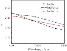
Here s is the refractive index of the substrate (1.5 for glass). Using Eqs. (3) and (4), we can obtain the refractive indices of the deposited samples, as illustrated in Fig. 9. It can be seen that, in the zone of transparency, all the refractive indices vary between 1.9 and 2.37, which are a little smaller than those reported in Ref. [22]. Besides, it can also be observed in Fig. 9 that the refractive index slightly decreases after either Ag or Sn doping.
The electrical properties of the deposited films are summarized in Table 2. The Hall measurement proves that all these samples are of n-type conductivity. Both the Ag and Sn dopings result in a reduction of the electrical resistivity and an increase of the carrier concentration. For Ag doping, the grain boundary scattering is reduced due to the considerable increase of the crystallite size induced by the doping. Since there is a high concentration of In vacancies in the In2S3 thin film, the Ag ions can be easily doped into the In sites serving as donors. As a result, doping with Ag leads to the rapid increase of the carrier concentration. For Sn doping, the vacant cationic sites might be occupied by Sn atoms, or the Sn atoms might replace the In atoms progressively.[10] As the Sn element belongs to group IV, whether it is in the substitutional position or in the interstitial position, it will act as a donor. Therefore, it will provide electrons and increase the electron concentration, thus promoting the conductivity.[23] The In2S3 buffer layers with low resistivity can reduce the series resistance of the solar cell, which will increase the short circuit current of the solar cell. Therefore, the Sn-doped In2S3 is more suitable for buffer layer application in solar cells concerning the electrical properties.
| Table 2. Electrical properties of the samples. |
We discussed the preparation and characterization of the Ag- and Sn-doped In2S3 films. The doping was realized by thermal diffusion. The structural, electrical, and optical properties of the deposited films were studied. All the deposited films showed a cubic β -In2S3 phase with a preferential growth direction along (311). XPS verified the incorporation of Ag and Sn into the In2S3 thin films. The optical properties showed that the Ag doping decreased the band gap while the Sn incorporation increased the band gap. Besides, both Ag and Sn dopings led to an improvement in carrier concentration and a significant decrease in resistivity. Since a wider band gap can promote the light transmission in the blue wavelength region and a buffer layer with low resistivity can reduce the series resistance of the solar cell, which will lead to a promotion in the short circuit current of the solar cell, the Sn-doped In2S3 thin film is more suitable for buffer layer application in solar cells.
| 1 |
|
| 2 |
|
| 3 |
|
| 4 |
|
| 5 |
|
| 6 |
|
| 7 |
|
| 8 |
|
| 9 |
|
| 10 |
|
| 11 |
|
| 12 |
|
| 13 |
|
| 14 |
|
| 15 |
|
| 16 |
|
| 17 |
|
| 18 |
|
| 19 |
|
| 20 |
|
| 21 |
|
| 22 |
|
| 23 |
|


