Modulation of WN x/Ge Schottky barrier height by varying N composition of tungsten nitride

Modulation of WN x/Ge Schottky barrier height by varying N composition of tungsten nitride |
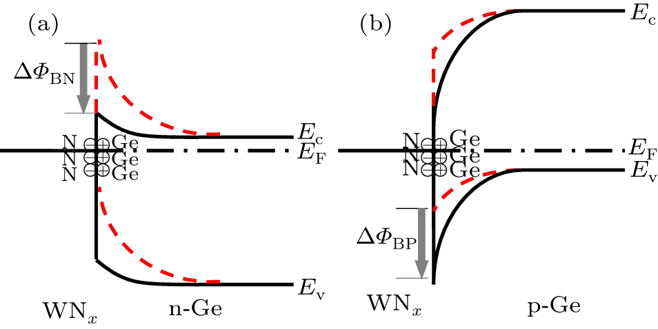
| Schematic band diagram of the pinning-alleviated WN x /n-Ge (a) and WN x /p-Ge (b) contacts by the interfacial dipoles layer. Here, E c is the conduction band edge, E v is the valence band edge, and E F is the Fermi level. |
 |