*Project supported by the National Natural Science Foundation of China (Grant No. 51272250), the National Basic Research Program of China (Grant No. 2011CBA00105), the National High Technology Research and Development Program of China (Grant No. 2014AA032702), and the Beijing Natural Science Foundation, China (Grant No. 2152035).
Abstract
We report the thickness dependence of critical current density ( Jc) in YBa2Cu3O7− x (YBCO) films with BaZrO3 (BZO) and Y2O3 additions grown on single crystal LaAlO3 substrates by metalorganic deposition using trifluoroacetates (TFA-MOD). Comparing with pure YBCO films, the Jc of BZO/Y2O3-doped YBCO films was significantly enhanced. It was also found that with the increase of the thickness of YBCO film from 0.25 μm to 1.5 μm, the Ic of BZO/Y2O3-doped YBCO film increased from 130 A/cm to 250 A/cm and yet Jc of YBCO film decreased from 6.5 MA/cm2 to 2.5 M A/cm2. The thick BZO/Y2O3-doped MOD-YBCO film showed lower Jc, which is mainly attributed to the formation of a-axis grains and pores.
Keyword:
74.78.−w; 74.25.Sv; YBa2Cu3O7− x films; thickness; BZO/Y2O3 doping; texture
YBa2Cu3O7− x (YBCO) is currently the most researched material for the second generation superconducting wire, and hopefully the best candidate material for electric power applications in motors, generators, transformers, fault current limiters, and superconducting magnetic energy storage requiring high critical currents (Ic) at 77 K. An obvious way to obtain high Ic is to increase the thickness of the superconducting YBCO layer. However, the critical current density (Jc) decreases rapidly as the YBCO thickness is increased. Whether this reduction is due to inherent vortex physics or thickness dependent material microstructure is still not thoroughly understood. As for the investigation of the mechanism of thickness dependence of the Jc in YBCO films, much work has been reported in recent years.[1– 15] In contrast, only a few successful examples depositing thick YBCO films with high performance have been reported. In 1999, Foltyn et al.[16] considered that the possible reasons for Jc thickness dependence are the impurity diffusion from the substrate to contaminate the YBCO layer nearest the interface, microstructural evolution in the form of degradation of crystallinity, and increasing surface roughness and microporosity. In 2002, Jia et al.[17] first demonstrated a multilayer architecture to enhance the supercurrent carrying capability of thick PLD-YBCO films. In that work, the interlayer of CeO2 reduced the structural defects induced during the increase of YBCO layer thickness and provided a starting template for growth of the subsequent high-quality YBCO layer. In 2005, Foltyn et al.[18] improved above-mentioned process and achieved 1400 A· cm− 1 (75.5 K) in a 3.5-μ m-YBCO film thick consisting of six YBCO layers interleaved with five CeO2 layers. In 2009, Zhou et al.[19] obtained Ic− w values of 400 A· cm− 1 at 1 T and 75.5 K in a 9-μ m-thick YBCO film with BZO and Y2O3 additions. According to their research group’ s experience, Feldmann et al. demonstrated a multilayer that combines the benefits of the multilayer architecture with the pinning enhancements of BZO/Y2O3 additions in 2010.[20] The 1000 A· cm− 1 was achieved in a single-layer 2.0-μ m-thick YBCO film, with a corresponding Jc value of 5.2 MA· cm− 2. Although these results are very valuable on understanding the mechanism of Jc thickness dependence, all these YBCO films were prepared by pulsed laser deposition (PLD), and there is increasing evidence that ex situ and in situ methods are not fully equivalent. In conventional TFA-MOD process, the thermal decomposition of TFA precursor films results in drastic reduction in film thickness and is accompanied by an increase of internal stress in the films during the pyrolysis process. Therefore, it is difficult to fabricate thick YBCO films by TFA-MOD process.[21]
In this work, a series of BZO/Y2O3-doped YBCO films with different thicknesses by TFA-MOD were successfully prepared, and the thickness dependence of superconducting property of BZO/Y2O3-doped YBCO films was investigated.
2. Experimental details
All BZO/Y2O3-doped YBCO films were prepared by TFA-MOD. The thickness of YBCO films varied from 250 nm to 15 μ m by changing precursor solution concentration and coating numbers. The substrates were single crystals of LaAlO3 (LAO). The precursor solution for BZO/Y2O3-doped YBCO film was prepared by dissolving the acetates of yttrium, barium and copper and Zr acetylacetonate with stoichiometric proportions in de-ionized water with an excess stoichiometric quantity of trifluoroacetic acid at room temperature. The resulting aqueous solution was refluxed for 10 h and then dried to a semisolid state, and then re-dissolved in methanol for drying. Finally, the residue was dissolved in appropriate methanol to get the final trifluoroacetate precursor solution with a concentration of 1.5– 3.0 mol/L. The solution was coated onto LAO substrates at a spinning rate of 3000 rpm for 2 min. Then the samples were put in a quartz tube within a horizontal furnace. Then the samples were put in a quartz tube within a horizontal furnace. Coated films were calcined at the temperature up to 400 ° C in 4.2% humidified oxygen with a flow rate of 500 cc/min. The calcined films were fired at 820 ° C with 4.2% humidified Ar gas mixed with 200 ppm oxygen gas for 3– 6 h and finally oxygenated at 500 ° C for 1.5– 3 h in pure oxygen gas atmosphere. Consequently, YBCO films consisting of BZO and Y2O3 with different thicknesses were obtained.
The film thickness was measured with a Dektak step profiler. The surface morphology of YBCO film was observed by field emission scanning electron microscopy (FESEM, FEI-Siron). The phase and texture of the as-grown film was characterized by x-ray diffraction (XRD) using Cu Kα radiation (Philips X’ Pert MRD). Resistive Ic values were measured by a standard four-probe method and Jc values in self field were measured by Jc-scan Leipzig system.
3. Results and discussion
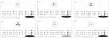
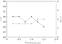
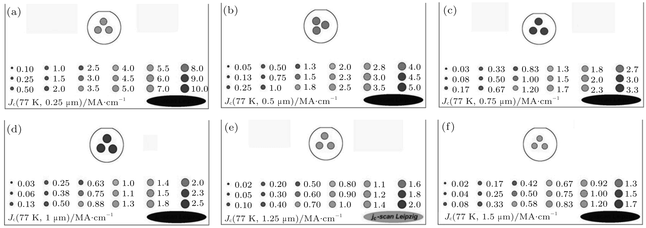
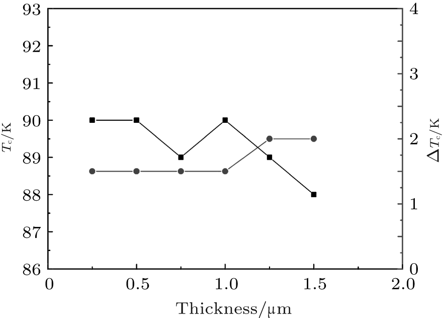
The critical current density (Jc) of the YBCO films were measured by the Jc-scan Leipzig system developed by the University of Leipzig, as shown in Fig. 1. The self-field Jc value for the BZO/Y2O3-doped YBCO film was 6.0 MA/cm2, which is much larger than the Jc value 3.0 MA/cm2 of pure YBCO films. It can also be clearly seen that Jc of BZO/Y2O3-doped YBCO film is largely dependent on the thickness under the optimized deposition conditions. With the increase of the thickness of YBCO film from 0.25 μ m to 1.5 μ m, the Jc decreases from 6.0 MA/cm2 to 0.75 MA/cm2. However, the critical current Ic increases with increasing the thickness of YBCO film from 0.25 μ m to 1.0 μ m. (The critical current is calculated from Ic= Jct, t is the thickness of YBCO films.) The 1.0-μ m-thick YBCO film has the highest Ic of 250 A/cm and Jc of 2.5 MA/cm2. After that with increasing the thickness, both the Jc and Ic values drop quickly. The Jc of the 1.5-μ m-thick YBCO film dropped to 0.75 MA/cm2. Tc values of YBCO samples were measured by the four probe method, as shown in Fig. 2. The Tc values of BZO/Y2O3-doped YBCO film with different thicknesses are between 90 K and 88 K, indicating that there is little effect of thickness on these solution-derived YBCO composite films. Moreover, the transition widths (Δ T) of these YBCO films were all lower than 2 K, which suggests the high homogeneity within the samples.
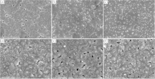
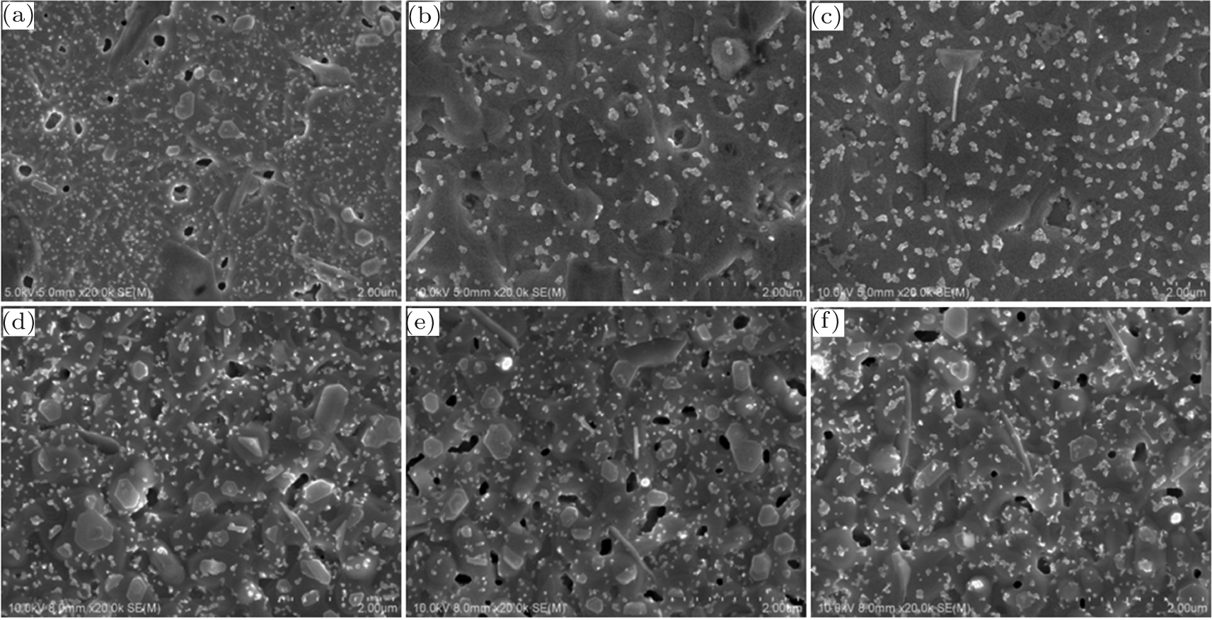
Figure 3 shows plan-view SEM images of the original top surfaces of BZO/Y2O3-doped MOD-YBCO films at thicknesses of 0.25, 0.5, 0.75, 1.0, 1.25, and 1.5 μ m. It can be seen that their surface morphologies were very similar with each other. A smooth surface was observed for all the samples. It differs from the morphology of YBCO films prepared by pulsed laser deposition (PLD). For mostly on in situ PLD– YBCO films, the grain and grain boundary of YBCO film becomes much rougher as thickness increases, [17] and even
Fig. 1. The critical current density in self field at 77 K for BZO/Y2O3-doped MOD-YBCO films with different thicknesses: (a) 0.25 μ m, (b)0.50 μ m, (c) 0.75 μ m, (d) 1.0 μ m, (e) 1.25 μ m, (f) 1.50 μ m.
some cracks appear in PLD-YBCO films. These results indicated that a rougher surface is not related to the Jc drop for BZO/Y2O3-doped MOD-YBCO films. It can also be seen that many nanoparticles appear in the whole area of our samples. These nanoparticles have been demonstrated to be the Y2O3 and BaZrO3 phases, [22] and for the 1.25-μ m-thick YBCO film, few needle (a-axis) grains appeared in the YBCO films, as the arrow labeled in Fig. 1(e) Furthermore, it can be seen from Fig. 1(f) that more a-axis grains are easily identified due to their platelet-like shape and their orientation parallel to the orthogonal (100) axes of the substrate, and some pores can be seen for thick YBCO films.
Fig. 2. Dependence of critical temperature (Tc and Δ Tc) on the thickness for BZO/Y2O3-doped MOD-YBCO films.
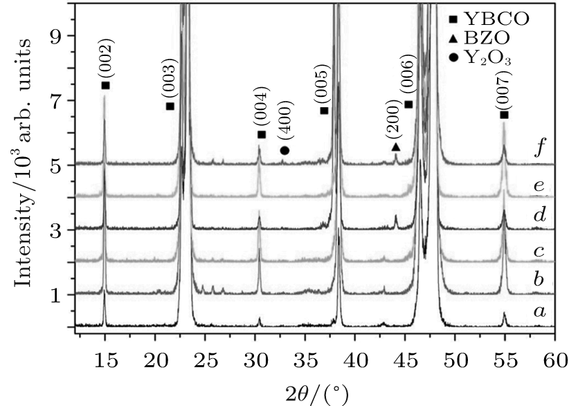
Figure 4 shows the XRD θ – 2θ diffraction patterns for the same samples as in Fig. 3. It can be seen that all the samples with different thicknesses have similar crystal phases and structures. The major diffraction peaks for all the samples can be indexed as (00l) reflections of YBCO phase, which indicates a well-textured, c-axis oriented YBCO grain structure, and the weak peaks at 2θ angles of 43.238° and 57.660° are assigned to the BZO (200) phase and Y2O3 (622), respectively. It demonstrates that the YBCO film prepared using the excess acetates of yttrium and Zr acetylacetonate TFA precursor solution formed BZO and Y2O3 phases. All the samples with different thicknesses are completely crystallized with YBCO (00l) phase. Furthermore, we can observe that the intensity of YBCO diffraction peaks with increasing thickness remain substantially unchanged. In addition, for BZO/Y2O3-doped MOD-YBCO films with thicknesses of 1.25 μ m and 1.5 μ m, there is one weak peak at 2θ angles of 23.261° , which can be indexed to the YBCO (100) phase (not shown in the manuscript). It can be concluded that the YBCO a-axis grain emerges when the thickness is higher than 1.25 μ m.
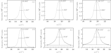
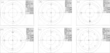
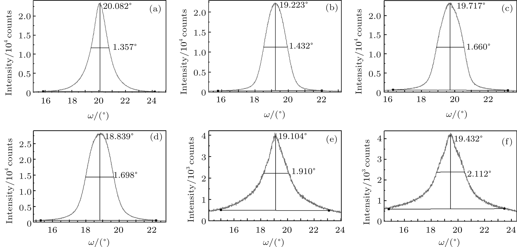
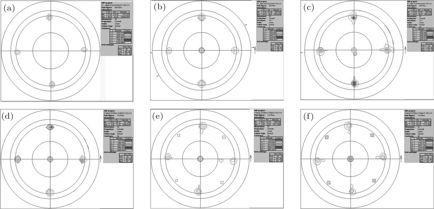
For further evaluation the texture of all the samples, x-ray (005) ω -scan and the (102) pole-figure were performed, as shown in Figs. 5 and 6. The full-width-half-maximums (FWHMs) of the out-of-plane texture were measured to be 1.367° , 1.432° , 1.660° , 1.698° , 1.910° , and 2.112° for the BZO/Y2O3-doped MOD-YBCO films at thicknesses of 0.25, 0.5, 0.75, 1.0, 1.25, and 1.5 μ m, respectively. It indicates that the BZO/Y2O3-doped MOD-YBCO films with the thickness less than 1.0 μ m have a better out-of-plane texture. From Figs. 6(a)– 6(d), a fourfold symmetry can be clearly seen, which confirms the BZO/Y2O3-doped MOD-YBCO films with the thickness less than 1.0 μ m present primarily a single in-plane orientation. However, it can be seen from Fig. 3(e) and Fig. 3(f) that there are four symmetric (100) YBCO reflections besides four symmetric (001) YBCO reflections. It is concluded that the BZO/Y2O3-doped MOD-YBCO films with
Fig. 3. SEM images of BZO/Y2O3-doped MOD-YBCO films revealing the surface morphology variation at thicknesses of 0.25, 0.5, 0.75, 1.0, 1.25, and 1.5 μ m ((a)– (f)); the scales for all images are the same.
thickness higher than 1.25 μ m have a-axis grains. The results agree well with the SEM and XRD θ – 2θ diffraction patterns analysis. Combining with Figs. 1 and 2, it is evident that the critical temperature of BZO/Y2O3-doped MOD-YBCO films is not affected by the texture and microstructure. However, the critical current density of BZO/Y2O3-doped MOD-YBCO films is very sensitive to texture and surface morphology. The BZO/Y2O3-doped MOD-YBCO films with thickness less than 1.0 μ m have a higher Jc value which is attributed to the formation of a stronger biaxial texture and dense surface. The samples with thickness higher than 1.25 μ m have a lower Jc value due to a-axis grains, poor biaxial texture and pores.
Fig. 4. XRD θ – 2θ diffraction patterns of the BZO/Y2O3-doped MOD-YBCO films with different thicknesses. Curves a– f: 0.25 μ m, 0.50 μ m, 0.75 μ m, 1.0 μ m, 1.25 μ m, 1.50 μ m.
Fig. 5. (005) ω -scan of the BZO/Y2O3-doped MOD-YBCO films with different thicknesses: (a) 0.25 μ m, (b) 0.50 μ m, (c) 0.75 μ m, (d) 1.0 μ m, (e) 1.25 μ m, (f) 1.50 μ m.
Fig. 6. Texture measurement of YBCO (102) on the BZO/Y2O3-doped MOD-YBCO films with different thicknesses: (a) 0.25 μ m, (b) 0.50 μ m, (c) 0.75 μ m (d)1.0 μ m, (e) 1.25 μ m, (f) 1.50 μ m.
4. Conclusion
The thick YBCO films with BZO and Y2O3 additions have been successfully fabricated by the TFA-MOD process. The thickness dependences of Jc and the microstructure of BZO/Y2O3-doped MOD-YBCO films were investigated. The Jc of BZO/Y2O3-doped MOD-YBCO films decreases from 6.0 MA/cm2 to 0.75 MA/cm2 and yet the Ic increases from 150 A/cm to 250 A/cm with increasing the thickness of MOD-YBCO films from 0.25 μ m to 1.0 μ m. When the thickness of YBCO film is further increased, the Jc and Ic of the YBCO films drop quickly. The a-axis grains, poor biaxial texture and many pores lead to damage of the superconducting property of BZO/Y2O3-doped MOD-YBCO thick films.
DamB, HuijbregtseJ M, KlaassenF C, Vand erGeest R C F, DoornbosG, RectorJ H, TestaA M, FreisemS, MartinezJ C, Stauble-PumpinB and GriessenR1999Nature399439DOI:10.1038/20880[Cited within:1][JCR: 38.597]
FeldmannD M, LarbalestierD C, FeenstraR, GapudA A, BudaiJ D, HolesingerT G and ArendtP N2003Appl. Phys. Lett. 833951DOI:10.1063/1.1625103[Cited within:1][JCR: 3.794]
AytugT, ParanthamanM, SpechtE D, ZhangY, KimK, ZuevY L, CantoniC, GoyalA, ChristenD K, MaroniV A and ChenY and Selvamanickam V2010Supercond. Sci. Technol. 23014005DOI:10.1088/0953-2048/23/1/014005[Cited within:1]
14
ZhaoS Q, LiuZ, ZhouY L, ChenZ H, LüH B, JinK J, ChengB L, YangG Z and WangS F2006Chin. Phys. B15444DOI:10.1088/1009-1963/15/2/035[Cited within:1][JCR: 1.148][CJCR: 1.2429]
15
DingF Z, GuH W, ZhangT, WangH Y, QuF, QiuQ Q, DaiS T and PengX Y2013Chin. Phys. B22077401DOI:10.1088/1674-1056/22/7/077401[Cited within:1][JCR: 1.148][CJCR: 1.2429]
16
FoltynS R, JiaQ X, ArendtP N, KinderL, FanY and SmithJ F1999Appl. Phys. Lett. 753692[Cited within:1][JCR: 3.794]
FoltynS R, WangH, CivaleL, JiaQ X, ArendtP N, MaiorovB, LiY, MaleyM P and MacManus-DriscollJ L2005Appl. Phys. Lett. 87162505DOI:10.1063/1.2106021[Cited within:1][JCR: 3.794]
19
ZhouH, MaiorovB, BailyS A, DowdenP C, KennisonJ A, StanL, HolesingerT G, JiaQ X, FoltynS R and CivaleL2009Supercond. Sci. Technol. 22085013DOI:10.1088/0953-2048/22/8/085013[Cited within:1]
20
FeldmannD M, HolesingerT G, MaiorovB, ZhouH, FoltynS R, CoulterJ Y and Apodoca2010Supercond. Sci. Technol. 23115016DOI:10.1088/0953-2048/23/11/115016[Cited within:1]
... 15] In contrast, only a few successful examples depositing thick YBCO films with high performance have been reported ...
1
1999
3.794
0.0
... [16] considered that the possible reasons for Jc thickness dependence are the impurity diffusion from the substrate to contaminate the YBCO layer nearest the interface, microstructural evolution in the form of degradation of crystallinity, and increasing surface roughness and microporosity ...
2
2002
3.794
0.0
... [17] first demonstrated a multilayer architecture to enhance the supercurrent carrying capability of thick PLD-YBCO films ...
... YBCO films, the grain and grain boundary of YBCO film becomes much rougher as thickness increases,[17] and even ...
1
2005
3.794
0.0
... [18] improved above-mentioned process and achieved 1400 A#cod#x00B7 ...
1
2009
0.0
0.0
... [19] obtained Ic#cod#x2212 ...
1
2010
0.0
0.0
... [20] The 1000 A#cod#x00B7 ...
1
2011
0.718
0.0
... [21] ...
1
2012
2.39
0.0
... These nanoparticles have been demonstrated to be the Y2O3 and BaZrO3 phases,[22] and for the 1 ...
Effects of thickness on superconducting properties and structures of Y2O3/BZO-doped MOD-YBCO films*


 , Gu Hong-Wei‡