Optical properties of rubrene thin film prepared by thermal evaporation*
[Chen Liang, Deng Jin-Xiang† , Kong Le, Cui Min, Chen Ren-Gang, Zhang Zi-Jia]
, Kong Le, Cui Min, Chen Ren-Gang, Zhang Zi-Jia]
|
|


†Corresponding author. E-mail: jdeng@bjut.edu.cn
*Project supported by the Funding for the Development Project of Beijing Municipal Education Commission of Science and Technology, China (Grant No. KZ201410005008), the Natural Science Foundation of Beijing City, China (Grant No. 4102014), and the Graduate Science Fund of the Beijing University of Technology, China (Grant No. ykj-2013-9835).
Rubrene thin films are deposited on quartz substrates and silver nanoparticles (Ag NPs) films by the thermal evaporation technique. The optical properties of rubrene thin film are investigated in a spectral range of 190 nm–1600 nm. The analysis of the absorption coefficient ( α) reveals direct allowed transition with a corresponding energy of 2.24 eV. The photoluminescence (PL) peak of the rubrene thin film is observed to be at 563 nm (2.21 eV). With the use of Ag NPs which are fabricated by radio-frequency (RF) magnetron sputtering on the quartz, the PL intensity is 8.5 times that of as-deposited rubrene thin film. It is attributed to the fact that the surface plasmon enhances the photoluminescence.
Rubrene (5, 6, 11, 12-tetraphenylnaphthacene) is a material that has drawn great interest because of its high electrical conductivity, high mobility, and emission characteristic. Rubrene thin film has been widely used in organic optoelectronic devices, such as the organic photovoltaic cell, [1, 2] thin film transistor (TFT), [3, 4] and organic light emitting diode (OLED).[5, 6] The study of characteristics of rubrene thin film is important for designing the optoelectronic devices. The optical properties are vital not only for understanding the optical transitions but also for numerically modeling the organic optoelectronic devices.[7– 9] The optical band gap (Eg) and absorption coefficient (α ) are the most significant parameters of thin films. The optical behavior of a material is utilized to determine its optical constants. Film is an ideal specimen for measuring the reflectance and transmittance. Therefore, an accurate measurement of the optical properties is extremely important. In this paper, firstly, we focus on the studies of the optical band gaps and optical constants of rubrene films by UV-visible spectrophotometry.
Rubrene has been extensively used in OLED.[5, 6] It is crucial to improve the luminous efficiency of rubrene thin film in its practical application. The emission intensity of luminophores of unit quantum yield can be increased by enhancing their absorption through increasing the local electric field.[10] Spectral overlap between the emission spectra of luminophores and the localized surface plasmon resonance (LSPR) spectrum of metal nanoparticles are very important for optimum luminescence enhancement.[11, 12] In this article it is also demonstrated that PL intensity of rubrene thin film can be enhanced by Ag NPs prepared by RF magnetron sputtering.
In this study, quartz glasses are used as substrates for optical measurement because of their low absorptions at UV-visible wavelengths. The substrates were cleaned in trichloroethylene, methanol, and acetone for 15 min in sequence with an ultrasonic cleaner. Then they were cleaned with deionized water and dried in N2 gas.
The deposition of the Ag NPs on the quartz substrates was carried out by RF magnetron sputtering using a high-purity Ag target (99.999%) with plasma generated by high-purity Ar (99.999%) at a substrate temperature of 200 ° C. The base pressure in the vacuum chamber was about 1.7× 10− 3 Pa. During sputtering, the pure Ar was introduced into the sputtering chamber, and the working pressure was maintained at 0.9 Pa. The Ag NPs thin films were grown for 5 s with RF powers of 40 W, 60 W, and 80 W respectively.
A 50-nm thin layer of rubrene was deposited on the top of Ag NPs thin film and blank quartz substrate by thermal evaporation in a high vacuum chamber with a base pressure of 5× 10− 4 Pa. The substrates were maintained at 90 ° C in the entire deposition process, which is the favorable temperature for the polycrystallization of the rubrene film.[1, 3] The depositions were performed at a low rate of 0.01 nm/s and measured in situ with a calibrated quartz thickness monitor.
The UV-visible-NIR transmittance and reflectance spectra were measured each as a function of the incident photon wavelength between 190 nm and 1600 nm with a Shimadzu UV-3600 spectrophotometer. The surface morphology was investigated by an FEI Quanta 600F atomic force microscope (AFM). The measurement of the PL intensity was carried out by a fluorescence spectrophotometer FLS920 at room temperature (RT). The excitation wavelength was 470 nm from an Xe lamp source (220 W).
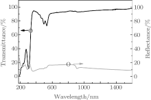
The transmittance (T) and reflectance (R) spectra of the rubrene thin film prepared on the quartz are shown in Fig. 1. They are measured for the normal incidence of light in the spectral range 190 nm– 1600 nm at room temperature. The use of transmission and reflection spectra is an important method to calculate the rubrene thin film absorption coefficient (α ) and optical band gap (Eg).
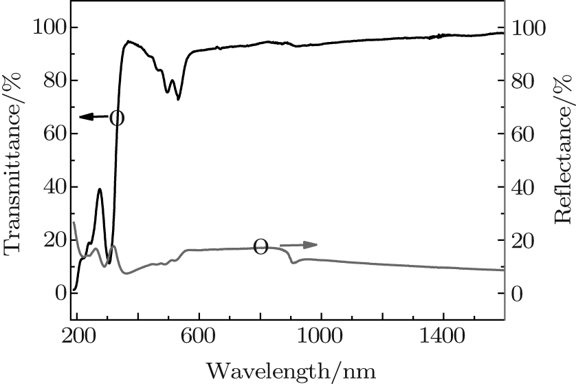 | Fig. 1. Transmission and reflection spectra of the rubrene thin film prepared on quartz. They are measured for the normal incidence of light in a spectral range of 190 nm– 1600 nm at room temperature. |
The interference effect can be ignored when the incident light is perpendicular to the thin film and the thin film satisfies the condition of 2nd ≫ λ 0 (index of refraction (n), thickness of thin film (d), wavelength in a vacuum (λ 0)). The absorption coefficient (α ) can be analyzed by the relation[13]
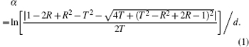
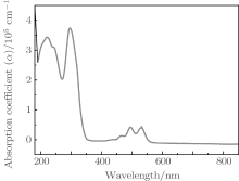
Figure 2 shows the α of the corresponding UV-visible spectrum of rubrene thin film. The rubrene film shows two significant peaks at 219 nm and 296 nm respectively. The distinct characterized peaks have generally been explained in terms of π – π * excitation from the highest occupied molecular orbital (HOMO) to the lowest unoccupied molecular orbital (LUMO) between bonding molecular orbital and antibonding molecular orbital.[14, 15] The first main transition at 296 nm is determined by the coefficient of HOMO– LUMO excitation and the excitation energy corresponding to the absorption maximum is 4.189 eV. The second transition occurring at 5.662 eV (219 nm) is an excitation from the HOMO to the LUMO. The intensity of the peak on the higher-wavelength side is weaker than that observed at the lower wavelength. There are two small peaks at 495 nm (2.505 eV) and 531 nm (2.335 eV) respectively. The rubrene absorption spectrum shows clear vibronic bands with a separation of about 0.17 eV, which can be attributed to C– C stretching vibration.[16] The minimum absorbance of rubrene thin film at the wavelength λ > 600 nm is shown in Fig. 2 and the light is hardly absorbed in that region.
 | Fig. 2. Absorption coefficient (α ) spectrum of rubrene thin film in the UV-visible spectral range. |
In many organic materials, it is usual to analyze the optical absorption at the fundamental edge in terms of band-to-band transitions theory.[15, 17] In this treatment, the absorption data follow a power-law behavior of Tauc[18] which is given by

where A is an energy-independent constant, hν is the photon energy, Eg is the optical band gap, and m values are assumed to be 1/2 and 2 for allowed direct, allowed indirect transitions, respectively.[9] Equation (2) can be rewritten as

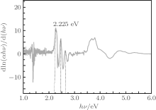
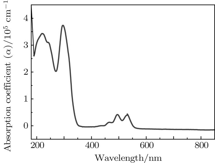
To determine the value of m, according to Eq. (3) the type of transition can be found. Figure 3 indicates the plot of d[ln(α hν )]/d(hν ) versus photon energy (hν ) of the rubrene thin film. The peaks at particular energy values give approximately the estimated optical band gap Eg of rubrene thin film in an energy region between 1.6 eV and 3.4 eV. In Fig. 3, the peaks have been determined to be at hν = Eg ≈ 2.225 near the fundamental absorption edge.
 | Fig. 3. Plot of photon energy (hν ) versus d[ln(α hν )]/d(hν ) of the rubrene thin film. |
Equation (1) can also be rewritten as

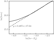
To find the value of parameter m, variation of ln(α hν ) with ln(hν – Eg) is plotted for the estimated values of Eg. The value of m is 0.487 from the slope of Fig. 4 for the estimated Eg value (2.225 eV). Therefore, 1/2 can be regarded as the value of m in Eq. (2). This suggests that the fundamental absorption edge in the rubrene thin film is formed by the direct-allowed transition.
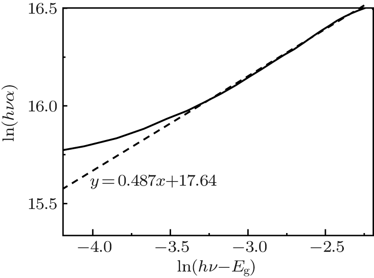 | Fig. 4. Plot of ln(α hν ) versus ln(hν – Eg) of the rubrene thin film. |
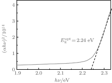
Optical band gap (Eg) is an important parameter describing the physical properties of material. It not only gives the basic absorption limit, but also reflects the optical band structure of a thin film. In order to obtain a more accurate value of the optical band gap of rubrene thin film, the plot of (α hν )2 versus hν of rubrene film is shown in Fig. 5. The intercept of the abscissa axis with the full line of the (α hν )2 versus hν plot allows the determination of the optical band gap (Eg). As shown in Fig. 5, the optical band gap value of the rubrene film is determined and the obtained value is 2.24 eV, which is in agreement with the deduced value above.
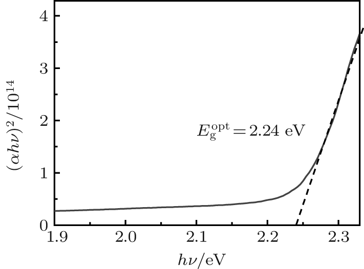 | Fig. 5. Plot of (α hν )2 versus hν of rubrene film. |
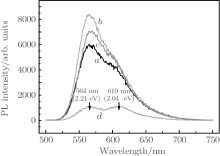
The PL peak of the rubrene thin film is observed at 563 nm (2.21 eV, yellowish green light emission) with an obvious shoulder peak at 610 nm (2.04 eV) as shown in Fig. 6(d). According to Ref. [19], the obvious emission peak of amorphous rubrene film should be near 560 nm, and the peak position of single crystalline rubrene is near 620 nm.[20] Based on these results, rubrene film can be regarded as a quite crystalline film embedded in the amorphous rubrene background.
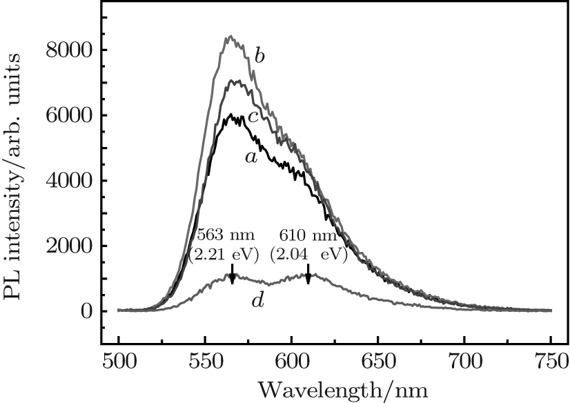 | Fig. 6. PL spectra of (curve d) rubrene and rubrene/Ag NPs thin films. The Ag NPs deposited on the quartz substrates with RF powers of (curve a) 40 W, (curve b) 60 W, and (curve c) 80 W. |
Curves a– c in Fig. 6 show the PL spectra of the rubrene/Ag NPs films. The Ag NPs are deposited on the quartz at a substrate temperature of 200 ° C for 5 s with RF powers of 40 W (curve a), 60 W (curve b), and 80 W (curve c). As the sputtering power successively increases, the PL intensity increases to a maximum, then decreases. The PL intensity is 8.5 times that of as-deposited rubrene thin film at a wavelength of 563 nm (2.21 eV) when the sputtering power is 60 W.
The PL intensity of rubrene/Ag NPs film shows a huge enhancement compared with that of as-deposited rubrene thin film. However, the PL spectra only have one broad band at 2.21 eV with a slight shoulder peak, which demonstrates that the crystal quality of the rubrene film is somewhat deteriorated when it is deposited on a Ag interlayer. Then it can be deduced that the crystal quality is not responsible for the giant enhancement of PL intensity.
The giant enhancement of PL intensity of the rubrene/Ag NPs can be explained by the fact that the surface plasmon enhances photoluminescence. Specifically, there are three reasons as follows. The first is the energy transfer effect in the SPR coupling. With light irradiation, free electrons on the surface of the Ag NPs oscillate collectively, which forms the surface plasmon (SP) absorption at 2.53 eV∼ 3.02 eV and induces polarization. A strong extinction of the incident light occurs at the SP frequency. It leads to the conclusion that Ag NPs absorb more energy from the incident light, and then transfer the energy to rubrene, as the SP band of Ag NPs approaches the photon-emission band of the rubrene thin film. Therefore, the energy transfer effect in the SPR coupling induces more excitons in the light-emitting rubrene thin film.[21, 22] The second reason is the SP-mediated emission, in which excitons are excited within the semiconductor coupled into the SP-modes at the metal/semiconductor interface when the emission energy of the semiconductor and the SP energy are similar. Then, exciton recombination produces SPs instead of photons, and this recombination path enhances the recombination rate. The coupled SP energy can be recovered as free space photons if the interface is sufficiently rough to scatter the SPs.[23] The last one is that the scattering efficiency is very high when the particle size is larger than 30 nm[24] for Ag colloids. The positive effect of the light scattering makes the absorption of light more efficient, which is indeed responsible for the enhancement of emission. Therefore, the enhanced emission of the rubrene/Ag NPs sample is observed from the PL measurements.
According to Mie theory, as the frequency of the incident photon is close to the surface plasmon oscillation frequency of metal nanoparticles, the photon will resonate with the surface conduction electrons and is strongly scattered or absorbed by the metal nanoparticles. For small particles in the quasi-static limit, the scattering and absorption cross sections are given by[22]

Here, α is the polarizability of the particle. When it is close to the frequency of surface plasmon resonance, light may interact with the particle over a cross-sectional area larger than the geometric cross section of the particle because the polarizability of the particle becomes very high in this frequency range.[25] Thus, transmittance decreases significantly at the position of surface plasmon resonance peak.
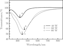
The transmission spectra of the Ag NPs which deposit on the quartz substrates at different RF powers of (curve a) 40 W, (curve b) 60 W, and (curve c) 80 W are presented in Fig. 7. The wavelengths of transmission peaks are 427 nm, 466 nm, and 447 nm respectively. The SPR wavelength shifts to a longer wavelength when the RF power is 60 W. When the emission energy of rubrene (2.21 eV, emission wavelength is 563 nm) approaches to the SP resonance energy of Ag NPs, it can be coupled into the SP modes. As a result, the enhanced emission is observed from the PL measurement of the metal-capped semiconductor. An 8.5-fold enhancement of the emission light is observed from the rubrene on Ag NPs which are deposited at 60 W, higher than those at the other RF powers.[26, 27]
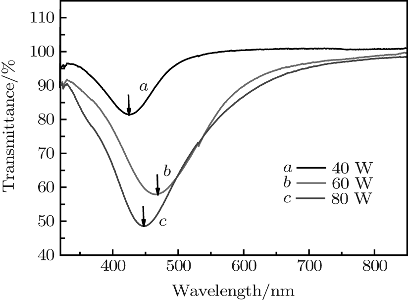 | Fig. 7. Transmission spectra of the Ag NPs deposited on the quartz substrates at a substrate temperature of 200 ° C for 5 s with RF powers of (curve a) 40 W, (curve b) 60 W, and (curve c) 80 W. The transmission peak wavelengths are 427 nm, 466 nm, and 447 nm respectively. |
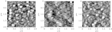
As SPR effects mainly depend on the particle size and the inter-particle distance, [28, 29] it is important to tune and optimize these parameters. The RF power is tuned to increase the spectral overlap between the emission spectra of rubrene and SPR spectra. The AFM images of the Ag NPs films deposited at RF powers of 40 W, 60 W, and 80 W are shown in Figs. 8(a)– 8(c). The average sizes are about 121.6 nm, 79.4 nm, and 179.2 nm respectively. It is apparent that particles deposited at 60 W are much smaller and less rougher than the other two samples.
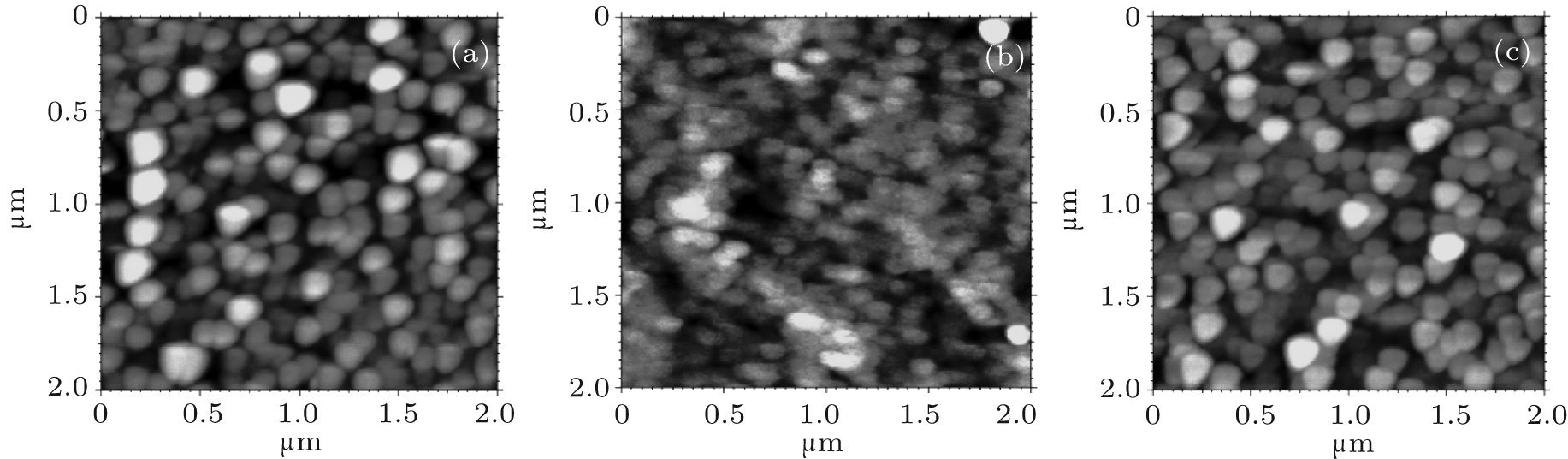 | Fig. 8. AFM of the Ag NPs deposited with the RF powers of (a) 40 W, (b) 60 W, and (c) 80 W. The fields of view (scan areas) of the images are 2.0 μ m× 2.0 μ m. |
At 40 W, more surface diffusion of atoms occurs significantly on the substrate. The small nanoparticles are able to migrate and relax to form nanoparticles with larger in-plane dimensions. When the sputtering power is 60 W, the number of atoms from the Ag target sputtered by Ar becomes larger per unit time, and the excess of atoms may not have sufficient time to migrate across the surface to combine with the formed Ag particle nuclei and promote their growth. Instead, more nuclei are formed. Hence, the Ag nanoparticle population density is higher. Since a higher density of nuclei can result in a higher population density of Ag NPs, the maximum size of the individual particles becomes limited.[30] When the RF power increases to 80 W, more atoms are sputtered. The Ag particles formed are larger than those at 60 W.
It is shown that the surface plasmon resonance wavelength increases with the metal particle size decreasing within a certain range.[28] Thus, an emission enhancement factor of 8.5 is demonstrated by the surface plasmon resonance wavelength approaching to the emission wavelengths of rubrene. Therefore, changing the sputtering power is a way to tune the particle size. The Ag NPs with smaller size and higher density show higher surface plasmon enhancement efficiency. Moreover, SPR wavelength can also be tuned by changing the sputtering time, substrate temperature, and the type of metal.
Rubrene thin film has been deposited on quartz by the thermal evaporation technique. The optical absorption coefficient and optical band gap are calculated by the transmission and reflection spectra in a range of 190 nm– 1600 nm. The analysis of the spectral behavior of the absorption coefficient (α ) in the absorption region reveals direct-allowed transition with a corresponding energy of 2.24 eV. The emission properties of the rubrene thin film and rubrene/Ag NPs film are investigated using photoluminescence spectroscopy, where the Ag NPs are fabricated by radio-frequency magnetron sputtering. The PL intensity of the rubrene/Ag NPs film is 8.5 times that of as-deposited rubrene thin film at a wavelength of 563 nm (2.21 eV). It is attributed to the effect of surface plasmon enhanced photoluminescence. The SPR energy of Ag NPs can be tuned to approach the emitted photon energy of rubrene by modifying the sputtering power, resulting in the enhancement of the PL efficiency.
| 1 |
|
| 2 |
|
| 3 |
|
| 4 |
|
| 5 |
|
| 6 |
|
| 7 |
|
| 8 |
|
| 9 |
|
| 10 |
|
| 11 |
|
| 12 |
|
| 13 |
|
| 14 |
|
| 15 |
|
| 16 |
|
| 17 |
|
| 18 |
|
| 19 |
|
| 20 |
|
| 21 |
|
| 22 |
|
| 23 |
|
| 24 |
|
| 25 |
|
| 26 |
|
| 27 |
|
| 28 |
|
| 29 |
|
| 30 |
|