Tunable coplanar waveguide resonator with nanowires

Tunable coplanar waveguide resonator with nanowires |
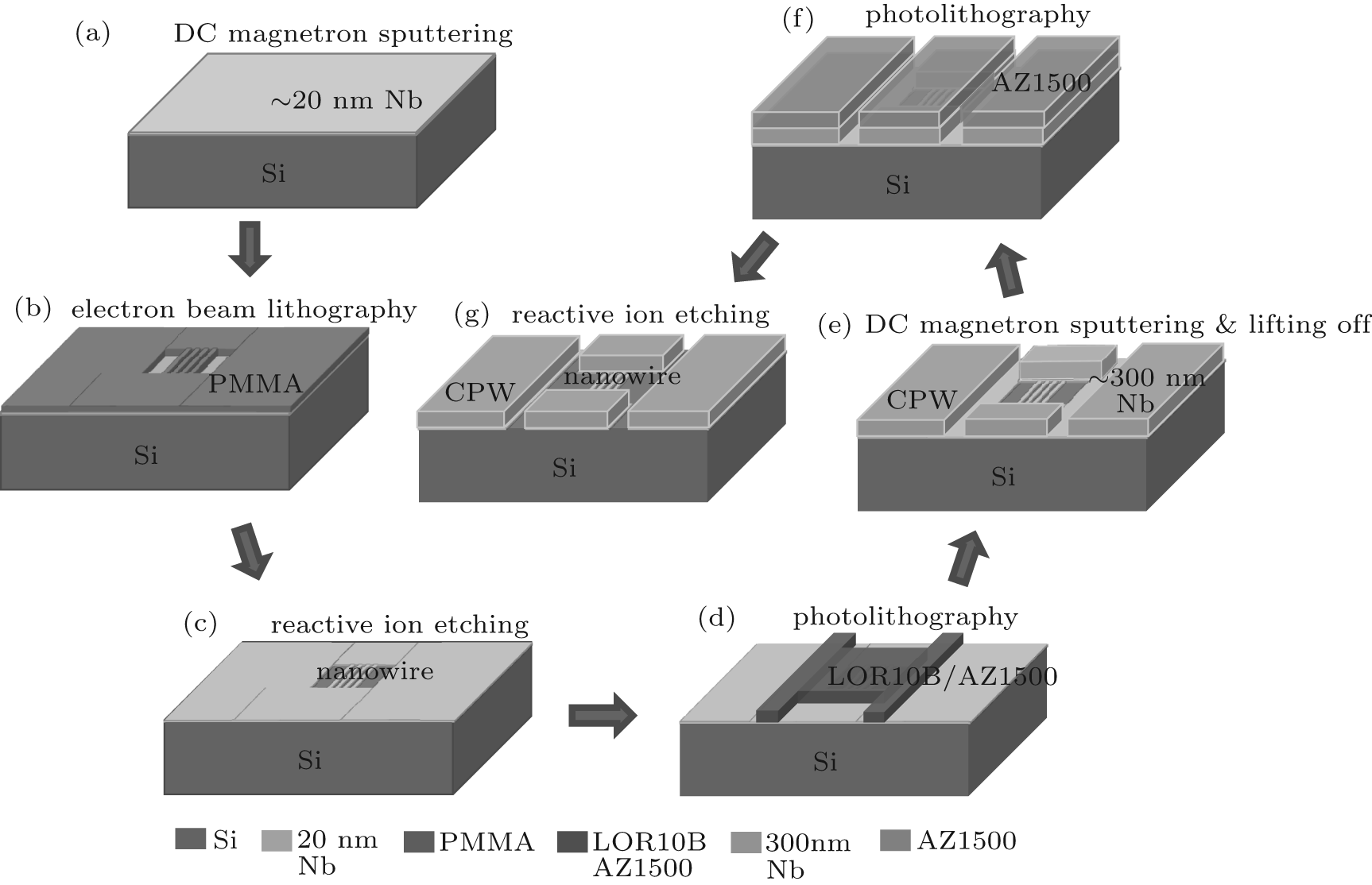
| Main steps of the fabrication process, from (a) to (g): (a) DC magnetron sputtering to deposit the first layer of ∼ 20-nm Nb film; (b) electron beam lithography to pattern the parallel nanowires; (c) reactive ion etching to transfer the nanowires to the thin Nb film; (d) photolithography to make the mask for CPWR; (e) DC magnetron sputtering and lifting off to deposit the second layer of ∼ 300-nm Nb film for CPWR; (f) photolithography to make the mask for the unneeded thin film between the center conductor and ground; (g) reactive ion etching to remove the unneeded thin film between the center conductor and ground. |
 |