Study on superstructure in ion co-doped BiFeO3 by using transmission electron microscopy*
[Pu Shi-Zhoua), b) , Guo Chaoa), b) , Li Mei-Yaa) , Chen Zhen-Lianc) , Zou Hua-Mina), b)†  ]
]
]
|
|


†Corresponding author. E-mail: hmzou@whu.edu.cn
*Project supported by the National Natural Science Foundation of China (Grant Nos. 51372174, 11074193, and 51132001) and the Fundamental Research Funds for the Central Universities.
La3+ and V5+ co-doped BiFeO3 ceramics are synthesized by rapid liquid sintering technique. The modulated structure in Bi0.85La0.15Fe0.97V0.03O3 is investigated by using transmission electron microscopy (TEM). Two kinds of superstructures are observed in the samples. One is the component modulated superstructure and twin-domain, which is generated by La3+ ordered substitution for Bi3+ and frequently appears. The chemical composition of the superstructure is explored by x-ray energy dispersive spectroscopy (EDS). The model of the ordered structure is proposed. Simulation based on the model is conducted. The second is the fluorite-type δ-Bi2O3 related superstructure. The relation between the ferroelectric property and the microstructure of the sample is also discussed.
Multiferroic materials, which exhibit the coexistence of ferroelectricity (FE), (anti)ferromagnetism (FM) and even ferroelasticity, have aroused great interest in recent years.[1– 4] The magnetoelectric coupling in the material allows designing new generation of devices with novel electronic properties, including data storage, actuators and transducers. Single phase BiFeO3 (BFO) is a multiferroic material which has high ferroelectric Curie temperature TC = 1103 K and anti-ferromagnetic Né el temperature TN = 643 K.[5] It has a non-centrosymmetric structure with R3c space group (a = 5.57874 Å , c = 13.8688 Å ).[6] The shifts of Bi and Fe along the threefold axis of ideal perovskite give rise to the spontaneous polarization.[7] BFO bulk reveals a disappointingly small value of spontaneous polarization (Ps = 6.1 μ C/cm2 along [111] direction[8]) compared with that of the FE polarization (Ps = 89.9 μ C/cm[4]) predicted by ab initio calculation, [9] which hinders its applications. Apart from the weak FE polarization and FM moment, the phase impurity and high leakage current are also the important factors which restrict the wide application of multiferroic materials.
It is believed that the space modulated spin structure of BFO can be collapsed by the A-site substitution resulting in a canted antiferromagnetic order, [10, 11] while the magnetic property of BFO could be modified by B-site doping.[12, 13] A lot of work has been done to improve the magnetic and ferroelectric properties of BFO bulks by doping. The remnant magnetization of 15% La-doped BFO is reported to be enhanced about 20 times as against pure BFO.[14] The dc resistance is increased by more than three orders of magnitude when 2% Fe3+ are substituted by Ti4+ in a BFO thin film.[15] Meanwhile, great efforts have been made to improve the purities of BFO ceramic by modifying the synthesizing process.[16, 17] Some BFO ceramics with high resistances are synthesized by the rapid liquid-phase sintering (RLPS) method, which implements fast heating, cooling treatments and short sintering time.[18] Unfortunately, most studies have focused only on the physical properties affected by the doping or processing of the sample. The study of the crystal structures of these ceramics was restricted to the measurement of x-ray diffraction, which only gives an average profile of the crystal structure. Few papers have paid attention to the micro-structure of the material and its effect on the physical properties. In fact, both a doping and sample processing technique can affect the crystal structure in two ways: making phase transition structurally for the whole crystal or producing defects in microstructure. The concentration and type of defects play a very important role in determining the properties of multiferroic material. A Monte Carlo simulation study revealed that the shape of hysteresis curve largely depends on defects.[19] The importance of defects in determining the properties of a ferroelectric has been verified experimentally.[20] The high leakage current in the sample is primarily caused by charge defects which are governed by Fe2+ ions, oxygen vacancies and bismuth vacancies.[21]
In this work, co-doped Bi1− xLaxFe1− yVyO3 samples are synthesized by the RLPS technique. One of the purposes of doping with high valence V5+ is to reduce oxygen vacancies. A V2O5 molecule might let two V5+ on the Fe sites 


The microstructure of Bi0.85La0.15Fe0.97V0.03O3 (BLFV) is investigated by transmission electron microscopy. The component modulated twin-domain generated by La3+ ordered substitution for Bi3+ is often observed in the BLFV sample. The twin structure is formed by the symmetrical array of modulation orientations about the twin boundary. The model and simulation for the superstructure are performed. A defect fluorite-type δ -Bi2O3 related superstructure which results from the ordering of oxygen vacancies can be found in all kinds of samples. This ordered structure might be associated with doping or/and sintering. The fluorite-type impure phase must be one of the reasons for the “ banana” -shaped polarization hysteresis loops.[22]
The investigated ceramics were prepared by an RLPS technique. The Bi2O3 (≥ 99.0%) (an excess Bi2O3 of 3 at.% to compensate for its evaporation), Fe2O3 (≥ 99.0%), La2O3(≥ 99.99%), and V2O5 (≥ 99.99%) powders were mixed in stoichiometric proportions for BLFV, respectively. The mixtures were milled by the ball milling for about 10 h at a rotation rate of 250 r/min. The mixtures were then pressed into disks with 15 mm in diameter and 1 mm in thickness, and dehydrated at 100 ° C for 24 h. After that, the pellets were sintered (with a fast heating rate) at 880 ° C for 7 min in air, and cooled down at a rapid rate of 40 ° /s.
The specimen for TEM observations were mechanically ground down to ∼ 30 μ m, and then further thinned by ion milling until it reached a thickness that can be penetrated by an electron beam in a TEM. The electron diffraction pattern (EDP) and high-resolution transmission electron microscopy (HRTEM) were performed on the JEOL-2010(HT) and JEOL-2010(FEF) electron microscopes, respectively. An x-ray energy dispersion spectroscopy (EDS) was also used on JEOL-2010(FEF). Both the TEM and the HRTEM were operated with an accelerating voltage of 200 kV at room temperature.
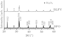
The average structure of the sample measured by x-ray diffraction (XRD) can be indexed as the rhombohedron with space group R3c (Fig. 1). The lattice distortion in BLVF is visible from the profile of XRD patterns compared with the profile of pure BFO. The lattice parameters calculated by Rietveld refinement method reveal that the co-doped BLVF undergoes a larger structure distortion than other samples, which were doped only on A or B site.[23]
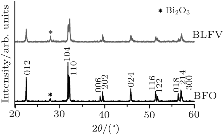 | Fig. 1. The x-ray diffraction profiles of BLFV sample (upper) and BFO (below) which is given for comparison. |
The selected area electron diffraction patterns were taken from BLFV. In order to obtain the three-dimensional information about the crystals, the specimen was tilted with respect to some fixed orientation. All of the reflections of the normal crystal grains can be indexed as rhombohedron. This is consistent with the result measured by x-ray.
Miller Index and the hexagonal coordinate system are adapted in the following description so as to conform with the transition matrix for superstructure and twins.
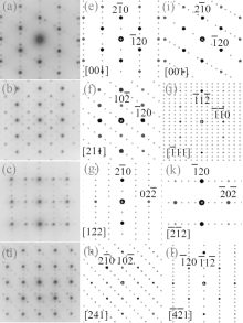
A superstructure can be easily found in some domains of co-doped BLVF samples. Figures 2(a)– 2(d) show the experimental EDPs taken from the same area of one grain. At the beginning, the EDPs in Figs. 2(a)– 2(d) are temporarily regarded as [001], [211], [122], and [241] zone axes, respectively. In each pattern, satellite spots can be obviously observed along two directions. According to the EDP viewed down alone [001], there seems to be two commensurately modulated wave vectors:


 | Fig. 2. (a)– (d) Experimental EDPs taken by tilting along two directions. (e)– (h) and (i)– (l) simulated EDPs, showing that the super-spots in the first column are the results of overlap of the corresponding patterns in the second column and the third column. |
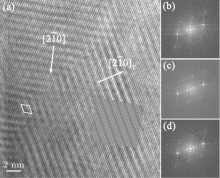
To fully understand the modulations, high-resolution transmission electron microscopy is used to characterize the BLVF sample. Figure 3(a) shows an HRTEM image taken from the area mentioned above along [001] zone axis. The modulated stripes are clearly seen, whose period is fourfold of the normal lattice period. It is interesting that the modulation of this area is divided into two parts, which are in fact along two different directions (denoted by white arrows). This can be proven by the Fourier transforms of different parts of the image, as displayed in Figs. 3(b) and 3(c). The angle between the two directions is 120° , which accords with that between q1 and q2. So, it is clear that the modulation wave vectors q1 and q2 in EDP of [001] zone axis come from different parts of the sample. Moreover, it is found by careful observation that the two parts can be regarded as “ twins” . Note that the “ twins’ here are not the twins in the normal sense because the lattice fringes are continuous all over the image, which indicates that the orientations of the crystal lattices of the two parts are identical, except that the modulation directions where the two parts lie symmetrically about the boundary. The twin relationship can be described as a 180° rotation around the twin axis [010], and the twin plane is

where (a, b, c) are the unit cell basis vectors of the matrix, and (aT, bT, cT) are those of the twin (subscript T denotes the symbol of twin). The transformation matrix of reciprocal vectors is the same as that of the unit cell basis vectors. Using this transformation matrix, one can obtain the relationship of the modulation wave vectors as follows:

This means that the modulation wave vector q2 in the twin is equivalent to that of q1 in the matrix. By this transformation, the zone axis 


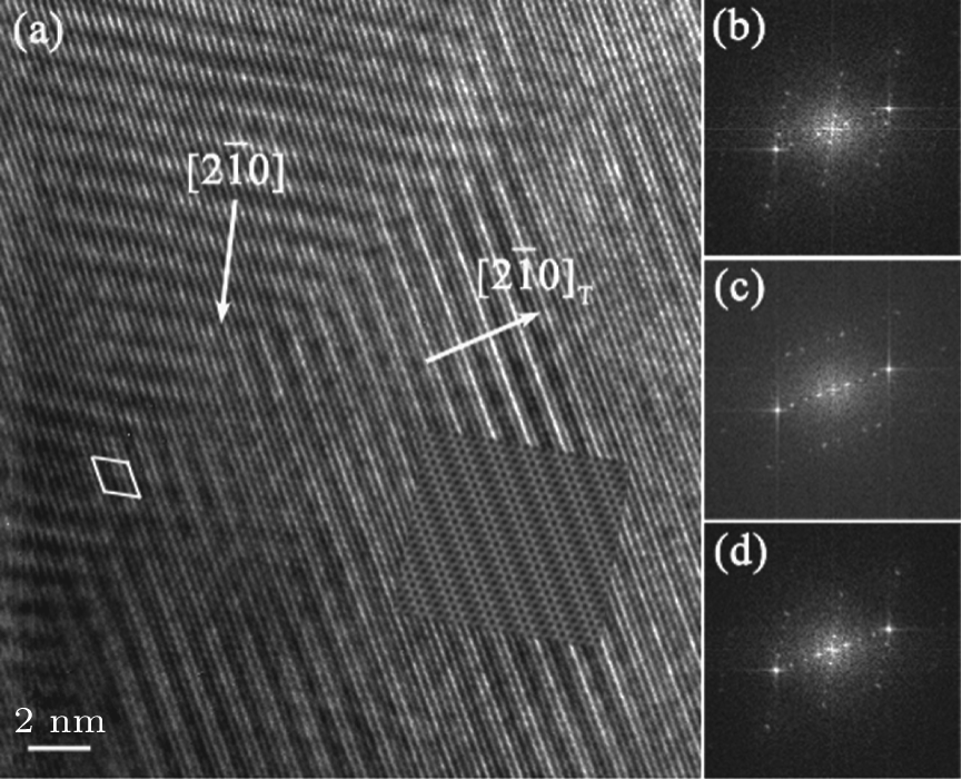 | Fig. 3. (a) HRTEM image of the modulated twin domain, and (b)– (d) the fast Fourier transforms of (b) upper left part, (c) lower right part, and (d) twin boundary of the image. The inset at the right bottom shows the simulated HRTEM image. The white parallelogrammical frame shows the projection of the supercell on (001) plane. |
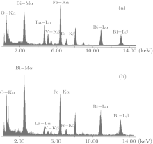
To investigate the origin of the modulation in BLFV, an EDS analysis is performed on a normal BLFV grain and the grain with a superstructure. The two profiles shown in Fig. 4 are normalized to the Fe– Kα peak at 6.4 keV. Compared with the EDS measurement data, the average ratio of La atoms with respect to the Bi and La atoms at A site is 15.6% for the normal grains (which is consistent with the nominal amount of doping), and it is 50.3% for the grains with the superstructure. The intensity of La– Lα peak at 4.6 keV in Fig. 4(a) is much higher than in Fig. 4(b). Furthermore, the intensity of Bi– Mα peak at 2.4 keV in Fig. 4(a) is lower than in Fig. 4(b). This implies that there are excess La atoms in the grain exhibiting the super spots in EDPs. It is noticed that the intensity of O– Kα peak in Fig. 4(a) is weaker than that in Fig. 4(b), which means that the content of oxygen in the superstructure is lower than that in the normal structure. This implies the oxygen vacancies existing in the superstructure. Considering the semi-quantitative characteristic of EDS analysis, several batches of samples are measured. The EDS data are collected at three to four positions even in one grain. All of the measurements give the same trend in that the concentration of La atoms in the grain with a superstructure is much higher than that in a normal grain. The data given above are the average of the data collected in one grain.
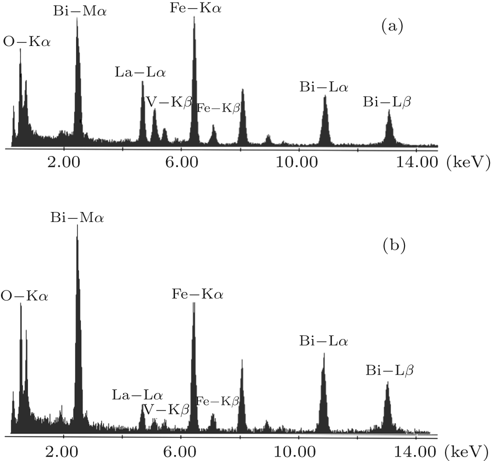 | Fig. 4. EDS spectrograms of grain with superstructure (a) and normal crystallite (b). Both of the profiles are normalized to the Fe– Kα peak at 6.4 keV. |
If the Bi3+ ions are orderly replaced by La3+ ions, modulated strips might appear in the HRTEM image. It is supposed that the Bi3+ cation are substituted by La3+ cation on one of every four 


where (a*, b*, c*) are the basis vectors of the reciprocal unit cell of the matrix.
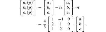
From the reciprocal unit cell, the superstructure unit cell in direct space can be derived as

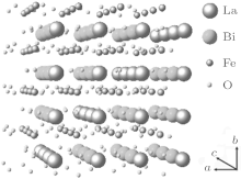
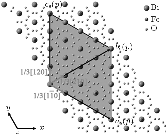
where (as, bs, cs) and (a, b, c) represent the basis vectors of the superlattice unit cell and the matrix unit cell in the hexagonal coordinate system, respectively. The unit cell of the superstructure can be regarded as a pseudocubic structure with a = b = c = 15.85 Å and α = β = γ = 90.0° , which is schematically shown in Fig. 5. In the unit cell, Bi3+ cations are replaced by La3+ cations on one of every four (012) and 
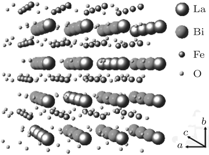 | Fig. 5. Diagram of the unit cell of the superstructure viewed along [001]. |
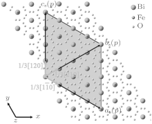
The supercell is projected on the (001) plane to verify the model of the superstructure. The matrix of the projection can be written as[24]
The shadowed parallelogram in Fig. 6 is the projection of the superstructure. The black arrows respectively denote the projections of the basis vectors of the supercell on (001) plane. The projection of the supercell is also marked in HRTEM in Fig. 3 with white frame.
 | Fig. 6. Projection of the superstructure unit cell on (001) plane. La atoms are not shown in the diagram. |
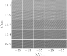
The simulations of HRTEM image along [001] zone axis and EDPs are conducted according to the model of a supercell. The simulation for HRTEM image is also performed in a defocus range from Δ f = − 50 nm to Δ f = 30 nm and a sample thickness range from t = 2.8 nm to t = 28 nm. Part of the simulated figures containing the best-fit ones are shown in Fig. 7. The image for Δ f = − 35 nm and t = 16.7 nm appears to be in good consistence with the experimental HRTEM image. The super reflection spots in the EDPs result from both the orderly substitution and the twin domains. The fact that simulated EDPs match the experimental patterns well is illustrated with Fig. 2.
 | Fig. 7. Simulated HRTEM images of the superstructure along [001] as a function of thickness and defocus value. |
There is another dopant V5+ in the BLFV sample. Why then is V5+ absent from the modulation? The amount of the dopant is as small as 3%. If V5+ orderly occupied the sites, there would be a much long period of the lattice. The long period in real space cannot form a reasonable period, which can be distinguished in reciprocal space. There exist few possibilities for V5+ to be orderly arranged in such a supercell.
In summary, the La3+ ions in the samples prepared with RLPS technique are unevenly distributed in the material. In the La3+ ion rich area, the La3+ ions tend to be distributed in a manner of long range ordering. HRTEM image shows the periodic stripes derived from the iron orderly arrangement. The content of La in the modulated grains is higher than that in the normal grains. The fact that the oxygen content in the superstructure is small might imply that there are oxygen vacancies in the superstructure.
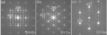
A kind of superstructure related to fluorite-type δ -Bi2O3 is also found in the BLFV sample. Figure 8 shows the EDPs of the crystallite viewed down along [010]F, [011]F, and [111]F directions. The subscript ‘ F’ represents that the zone axis is indexed according to the fluorite structure. The main spots in the EDPs can be indexed according to fluorite subcell with space group 
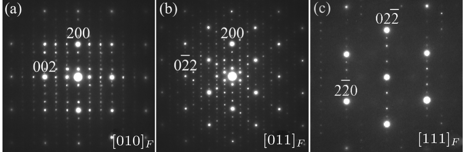 | Fig. 8. EDPs of superstructure associated with fluorite-type δ -Bi2O3 viewed down along (a) [010]F, (b) [011]F, and (c) [111]F direction. The subscript F indicates that the zone axis is indexed according to the fluorite structure. |
HRTEM and EDS are employed to further explore the occurrence of the super spots. It is suggested that the modulated structure might be induced by oxygen vacancies ordered. The dimension of the supercell is derived as 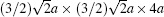
The ideal fluorite structure (CaF2) can be described as an oxygen cubic cage encapsulated inside a face-centered cubic cation lattice, in which each cation has eight coordinated anions and each anion has four coordinated cations. The δ -Bi2O3 is a high-temperature form of bismuth oxide with a defective fluorite-type structure. It can be stabilized at room temperature by being doped with rare earth cation or transition metal cation.[26] For δ -Bi2O3, only 75% oxygen sites are randomly occupied, and 25% oxygen sites are vacant, which leaves oxygen vacancies in the cation tetrahedron. A high rate of oxygen vacancies makes δ -Bi2O3 a good ion conductor. The EDS spectroscopy of the modulated grains gives the evidence of high concentration of oxygen vacancies.[22] The existence of fluorite-type δ -Bi2O3 related superstructure will cause a large leakage current in the BLFV sample. One of the key factors for the existence of the superstructure might be related to the processing of the sample. In the RLPS technique, the time of thermal process is limited to a time as short as several minutes, which is insufficient for the raw material to diffuse. Thus, a small amount of Fe2O3 reacts with Bi2O3 to form the superstructure before adequate Fe2O3 is combined to produce BiFeO3.
The microstructure of co-doped BiFeO3 ceramics synthesized by RLPS technique is investigated by TEM. Two kinds of superstructures can be easily found in the samples. One kind of modulated structure is derived from Bi3+ cation orderly substituted by La3+ cation. The other kind of structure is the δ -Bi2O3 related superstructure. These two kinds of superstructures might affect the ferroelectricity in two aspects. As is well known, the ferroelectricity of BiFeO3 comes mainly from the lone pair of electrons of Bi. The structural feature of BiFeO3 is a non-centrosymmetric unit cell. On the one hand, the ordered substitution gives rise to a pseudocubic superstructure unit cell and high concentration of La3+ . Furthermore, the symmetry of the superstructure is not a non-centrosymmetric. These might weaken the ferroelectricity of the material. On the other hand, both of the superstructures contain oxygen vacancies. Oxygen vacancy is one of the main sources of high leakage current in the sample. A high leakage current in the sample would result in “ banana” -shaped[27] polarization hysteresis loop. Further elaborate study reveals that the effect of oxygen vacancies would give rise to a pinched displacement-electric field hysteresis loop.[28]
| 1 |
|
| 2 |
|
| 3 |
|
| 4 |
|
| 5 |
|
| 6 |
|
| 7 |
|
| 8 |
|
| 9 |
|
| 10 |
|
| 11 |
|
| 12 |
|
| 13 |
|
| 14 |
|
| 15 |
|
| 16 |
|
| 17 |
|
| 18 |
|
| 19 |
|
| 20 |
|
| 21 |
|
| 22 |
|
| 23 |
|
| 24 |
|
| 25 |
|
| 26 |
|
| 27 |
|
| 28 |
|