Application of an Al-doped zinc oxide subcontact layer on vanadium-compensated 6H–SiC photoconductive switches

Application of an Al-doped zinc oxide subcontact layer on vanadium-compensated 6H–SiC photoconductive switches |
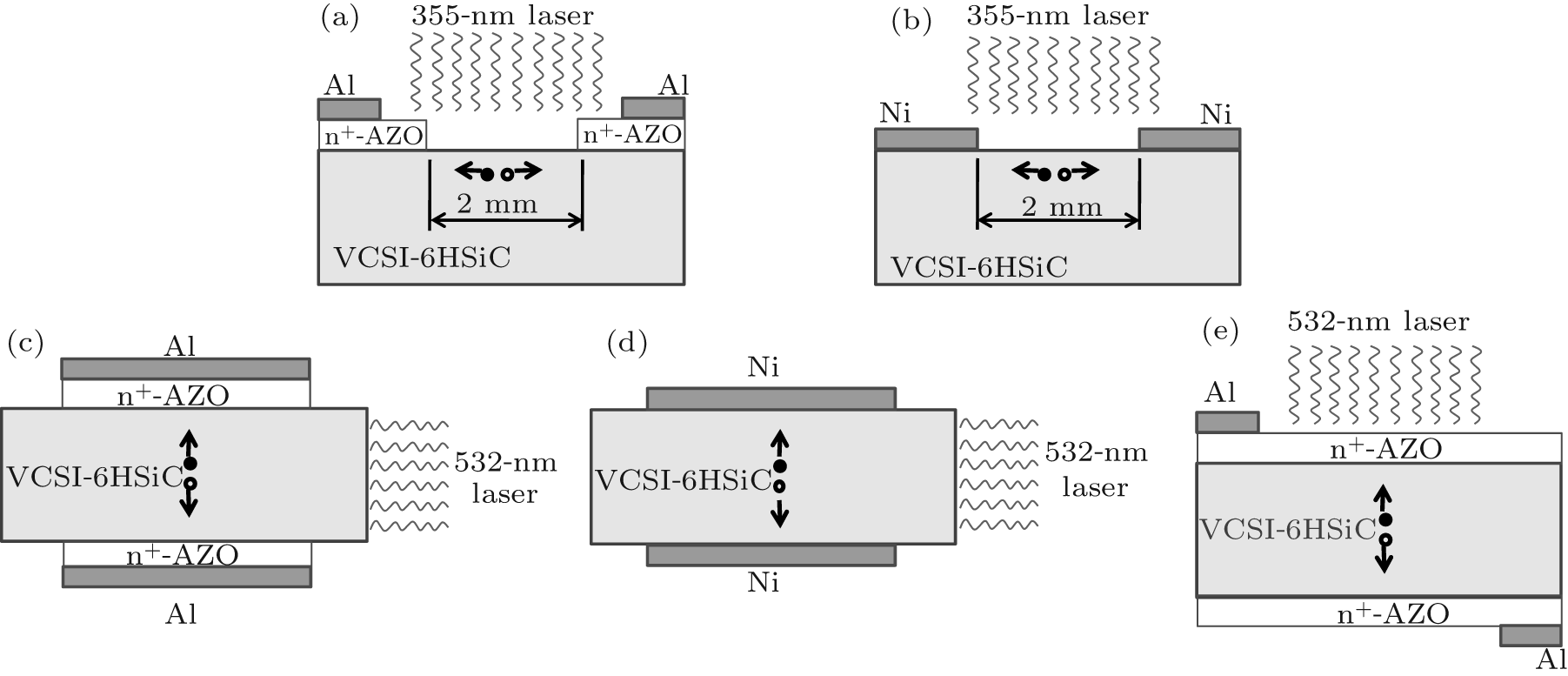
| Schematic diagram of lateral and vertical PCSSs: (a) PCSS-L1, (b) PCSS-L2, (c) PCSS-V1, (d) PCSS-V2, (e) PCSS-V3. |
 |