High performance silicon waveguide germanium photodetector
[Li Chonga), b)†  , Xue Chun-Lai
a) , Li Ya-Minga) , Li Chuan-Boa) , Cheng Bu-Wena) , Wang Qi-Minga) ]
, Xue Chun-Lai|
|


†Corresponding author. E-mail: chli@semi.ac.cn
High-performance Ge-on-SOI p–i–n waveguide photodetectors with different sizes were fabricated. The performances, in terms of dark-current, photo current responsivity and 3-dB bandwidth, were well studied. A responsivity of 0.842 A/W at 1550 nm and dark current of 70 nA was measured from this detector at -1 V. The detector with a size of 4 μm×10 μm demonstrated an optical band width of 19 GHz at -5 V for 1550 nm. Both the experimental results and the finite-difference time domain simulation show that, when the device size is above a certain threshold, the absorption is not sensitively dependent on such designing parameters as the width and length of the photodetector.
Since communication and sensor techniques have been greatly enhanced by the applications of optical signals, the improvement of integrated opto-electrical circuits allowing fast distribution and the processing of optical signal has becomes increasingly urgent. For metal-oxide-semiconductor (CMOS) integrated circuits (IC), silicon is the best choice as the substrate material due to its unique advantage in having metal interconnects compared with other conventional materials which would result in heat generation and limited bandwidth. Nowadays, optical communication is widely operated at wavelengths around 1550 nm, which shows the lowest fiber losses, or 1300 nm, which allows the lowest fiber dispersion. In order to achieve a better performance in integration with long-haul optical communication technology, a material with a larger absorption coefficient in the wavelength range of 1.30– 1.55 μ m is required. Germanium, which like silicon is a group IV material, has a very large optical absorption coefficient in the 1.30– 1.55 μ m wavelength range and it can also avoid the cross contamination with silicon unlike III– V materials. Therefore, a group IV photonic device, such as a Si/Ge photodetector, becomes increasingly important and has attracted great attention in recent years.[1– 7]
Compared with the compound semiconductors, group IV semiconductor materials show a lower absorption coefficient at the communication wavelength. Thus, a Si/Ge photodetector with a surface-normal illumination design often suffers from a trade-off issue between quantum efficiency and bandwidth, as demonstrated by many groups.[5– 7] However, this problem can be overcome by the integration of a waveguide in the photodetector since such a design can decouple the photon-absorption path and the carriers collection path, which is an essential factor for a well-designed Si/Ge photodetector. Since 2007 there have been many reports on waveguide-integrated germanium photodetectors; [1– 4] however, few attempts have been made to study the effects of the length and width of the photodetector on its optoelectronic performance.
In this paper we have built efficient germanium-on-silicon p– i– n waveguide photodetectors (Si/Ge-WG-PD) with a 0.5-μ m thickness of Ge film on silicon on insulator (SOI) substrate. The responsivity of photodetector is as high as 0.842 A/W at the wavelength of 1550 nm, and the dark current is 0.07 μ A at the reverse bias 1 V. For the detector size of 4 μ m× 10 μ m, a high bandwidth of 19 GHz at 3-dB is achieved at the wavelength of 1550 nm and the reverse bias is 5 V. A comparison of the performance of our Si/Ge waveguide photodetector with those from other groups is shown in Table 1, from which it is obvious that our Si/Ge photodetector has the best performance, especially in terms of its high responsivity and large bandwidth.
| Table 1. A comparison of the performance of our Si/Ge waveguide photodetector with those from other groups. |
In addition, Si/Ge waveguide photodetectors with different sizes were fabricated, and their absorption efficiency and dark current are compared, which shows that the absorption efficiency is independent of the length of the device when the length is above 10 μ m and not sensitive to the width of the device when the width is above 4 μ m. These conclusions are further confirmed by the finite-difference time domain (FDTD) simulation results.
A schematic diagram of the device structure is shown in Fig. 1(a), which explores the evanescent coupling technique. In this device, the intrinsic Ge absorption layer is integrated on top of the silicon waveguide to form a vertical-oriented p– i– n structure. The device is fabricated on a silicon substrate, which is followed with a 2-μ m-thick buried oxide layer and a 0.22-μ m-thick SOI wafer. Here, the buried oxide layer can confine the photo-absorption process within the photodetector more effectively than that only on a Si wafer, preventing optical leakage loss into the substrate and achieving higher quantum efficiency. The silicon waveguide was fabricated by etching a 100-nm-thick Si ridge with a width of 0.4 μ m, as shown in Fig. 1(b). After the fabrication of the silicon waveguide, the wafer was implanted with boron in the contact area of the top silicon surface with the end of the taper to form a p-type ohmic contact, and a rapid-thermal-annealing (RTA) process was followed to activate the dopant. Then, a Ge layer with a thickness of 500 nm was grown on top of the Si layer, and the width of the Ge waveguide was controlled by the window opening of the epitaxial growth. Phosphorus was implanted on top of the Ge film to form an n-type ohmic contact. After that, a 1200-nm-thick SiO2 passivation layer was deposited by plasma enhanced chemical vapor deposition (PECVD) at 300 ° C to insulate the mesa sidewall. The oxide widow for the pad contacts were opened by inductively couple plasma (ICP) etching separately. The metal contacts for both p- and n-type were formed by depositing and patterning a Ti/Al electrode on top of the doped area. The top view and SEM image of the WG-PD device are shown in Figs. 1(c) and 1(d), respectively.
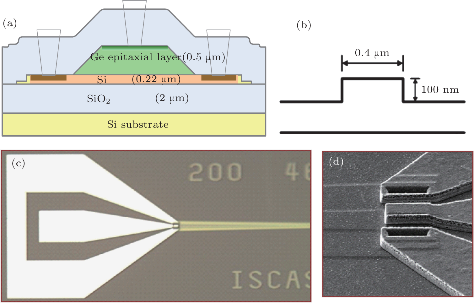 | Fig. 1. (a) A schematic diagram of the device structure: a vertical pin Ge waveguide photodetector integrated on top of a 0.22-μ m SOI waveguide. (b) A schematic diagram of the single-mode waveguide; (c) the top view of the device; (d) the SEM image of the WG-PD. |
The performance of the photodetector was characterized by its dark-current and photocurrent responsivity, and 3-dB bandwidth. For the dark-current characterization, the current– voltage characteristic of the device was measured by an Agilent B1500A semiconductor parameter analyzer on a probe station without any illumination at room temperature. For the photocurrent characterization, the current– voltage characteristic of the device was obtained with a laser radiation at the 1550 nm wavelength and a power of 0.7 mW. Here, the laser light was coupled into the silicon waveguide by a single-mode lensed optical fiber and the light output was measured by a calibrated detector.
Figure 2 shows the dark-current– voltage characteristics of the photodetectors with varying widths and lengths at room temperature. For the smallest photodetector (size: 4 μ m× 10 μ m), the dark current is 0.07 μ A at a reverse bias 1 V, i.e., a dark-current density of 175 mA/cm2. Practically, the dark current can be decreased further by more advanced Ge epitaxial growth technique, [8] the lateral wall quality of the Ge selective epitaxial layer and the quality of the surface passivation.
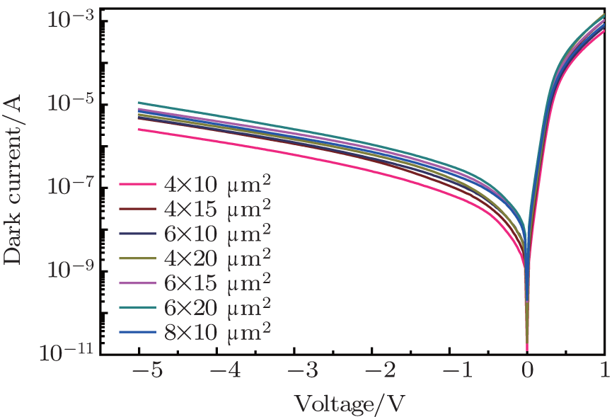 | Fig. 2. The dark-current– voltage characteristics of Si/Gep-i-n waveguide photodetectors with different sizes. |
Figure 3 shows the current– voltage characteristics of the device under laser radiation, in contrast with the dark-current response. There are two kinds of location of the top metal electrode, i.e., the n-type electrode of the device is either located on the center of the top mesa or around the edge of the mesa. Therefore, the influence coming from the difference in the locations of top electrode should be ruled out, such as Fig. 3(a). The photo current responsivity was calculated based on the total optical power incident on the photodetector, taking account of the transmission loss of the waveguide and the coupling loss caused by the optical fiber. Here, the propagation loss and taper loss of the waveguide were measured to be about 1.25 dB, and the coupling loss between the optical fiber and waveguide was measured to be about 4 dB. Therefore, the actual absorbed power for the detector was about 0.2 mW with an input power of 0.7 mW. For the photodetector with the size of 4 μ m× 10 μ m, the photo current is about 0.176 mA at a reverses bias of 1 V, i.e., the photocurrent responsivity of the detector is about 0.842 A/W at the 1550 nm wavelength. Correspondingly, the quantum efficiency was concluded as 68%. The current saturation at the zero bias indicates that this photodetector allows a complete photo-generated carrier collection even without any bias. In addition, the photocurrent responses with varying widths and lengths of the detectors are compared in Figs. 3(a) and 3(b), respectively, from which a similar responsivity is concluded for different widths and lengths of the detector. Therefore, we can conclude that the photocurrent response is less sensitive to the size of the detector when the width of the device is above 4 μ m and the length is above 10 μ m.
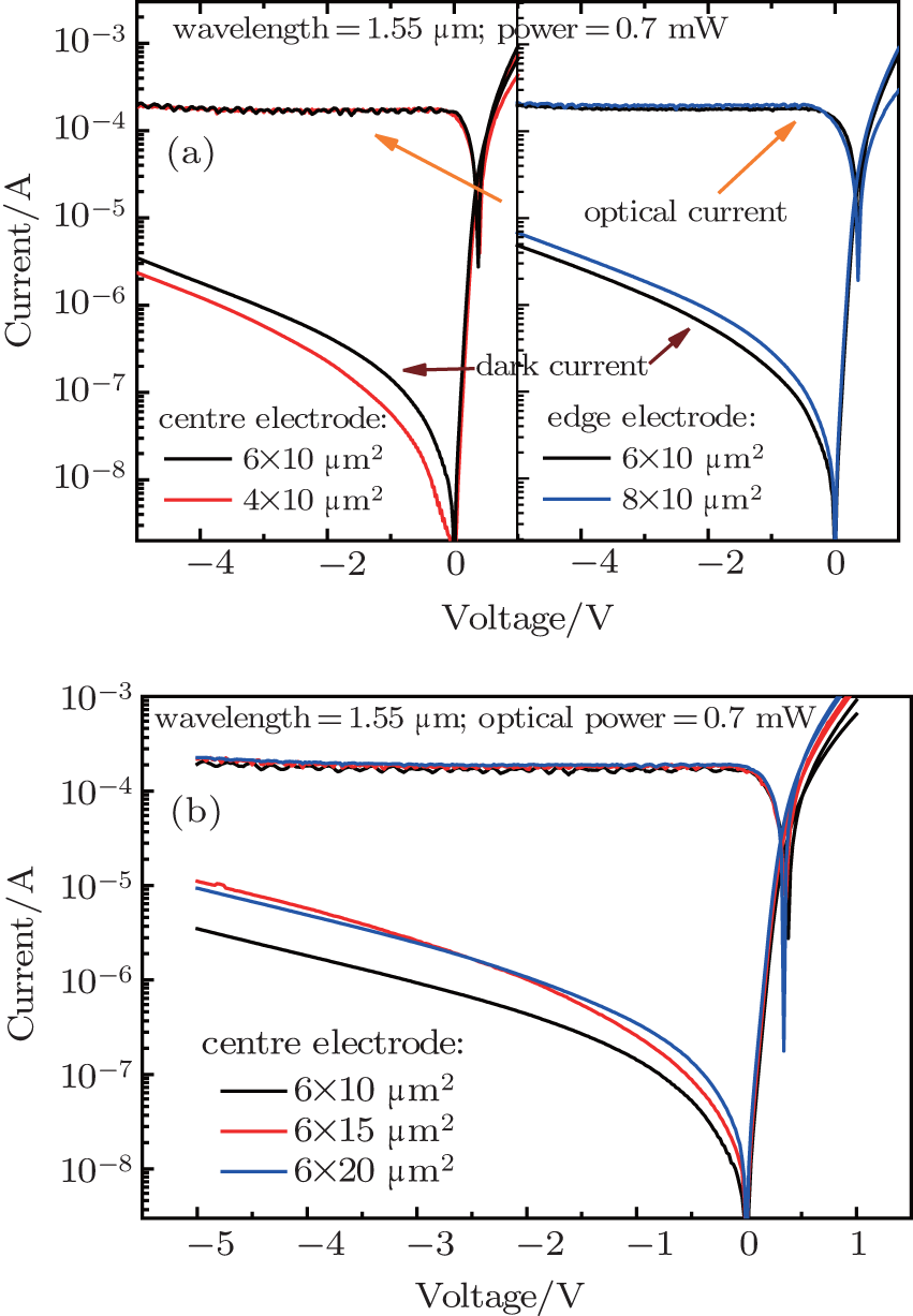 | Fig. 3. The current– voltage characteristics of the device without illumination and with laser radiation. (a) The devices with different widths, (b) the devices with different lengths. |
In order to provide theoretical evidence for the aforementioned conclusion about the photocurrent response, a three-dimensional finite difference time-domain (3D-FDTD) simulation of the same device structure is carried out. In this simulation, the refractive indexes of Ge, Si, and SiO2 at 1550 nm are adopted as 4.28, 3.48, and 1.46, respectively, and an absorption coefficient 4000/cm at 1550 nm is assumed for 0.13% tensile-strained Ge on Si.[9] In the FDTD analysis, the absorption efficient is defined as the ratio between absorbed optical power and input power. The simulation results are shown in Table 2, for different widths and lengths of detectors.
| Table 2. Results of the simulations for different widths and lengths of detectors. |
These simulation results on the absorption coefficients further confirm that the width and length of the photodetector have little influence on the absorption efficiency, which is consistent with our experimental results. Since these simulation results are based on an ideally modeled calculation, without considering any propagation loss in the waveguide, absorption loss of metal electrodes, scattering loss of the sidewall and other possible losses in the device, the simulation results generally show higher absorption efficiency than that concluded as expected from the experimental data.
These conclusions can be explained by the theory of evanescent wave absorption and taper loss. When the length of the device is greater than 10 μ m, the input optical power is almost totally absorbed by the Ge layer and the responsivity will float around a certain value. Moreover, the device width is equal to the wider end of the waveguide taper front of the photodetector. Theoretically, the responsivity with different widths should be different. However, the results from the experimental measurement and theoretical simulation indicate that the loss of the waveguide taper is too small to be recognized when the width of the device is above 2 μ m.
The response of the detector in the frequency domain was measured with a network analyzer in a range from 0.8 GHz to 30 GHz. The high-speed RF signal from the network analyzer was applied to an external modulator, which translates a steady optical source provided by a CW IR laser to a modulated signal with a 1550 nm wavelength and an average power of 0.5 mW. The modulated light was coupled into the waveguide by a single-mode fiber. A high-speed RF probe was used to collect the photo-generated carriers. The normalized frequency responses of the detector with an active area of 4 μ m× 10 μ m at different bias voltages are shown in Fig. 4. The measured 3-dB bandwidths at the voltage 0 V, − 1 V, − 3 V, and − 5 V are 0.28 GHz, 4.58 GHz, 16.64 GHz, and 19.00 GHz, respectively.
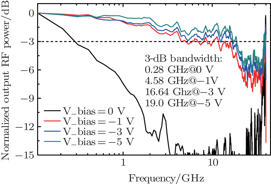 | Fig. 4. Normalized frequency responses at the wavelength 1550 nm for the detector with a size of 4 μ m× 10 μ m. |
Our further studies show that the frequency responsivity of the detector is limited by the slow diffusion of the carriers in the outside depletion layer, the carriers' transport through the depletion layer, and the load time of the capacitance and resistance. For the high frequency response, the transit time and the load time of the RC delay should be considered, especially when the thickness of the contact layers is thin enough for the diffusion time to be neglected.[10]
The transit time of the carriers in the intrinsic region is one limitation of the bandwidth, and is determined by the saturation drift velocity vsat (Ge: vsat = 6 × 106 cm/s) and the thickness of the intrinsic layer di. The carrier transit frequency fT can be calculated by[11]

Therefore, the transit time is estimated to be around 57.3 GHz. For a large fT, the absorption layer has to be as thin as possible in order to achieve a large intrinsic capacitance.
The RC delay of the detector is another limitation of the bandwidth. Ideally, the capacitance equals the intrinsic depletion capacitance, so the RC bandwidth fRC can be calculated by
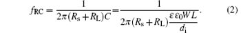
Here, RL is the load resistance (50 Ω in this case), Rs is the series resistance, L and W are the length and width of the photodetector, ɛ and ɛ 0 are the relative and vacuum permittivity, and di is the thickness of intrinsic zone. The intrinsic depletion capacitance is about 14.34 fF for the detector with di = 0.4 μ m, W = 4 μ m, and L = 10 μ m. From the semi-log plot of the current– voltage curve, the series resistance can be concluded at the region where the current deviates from the exponential increasing as Rs = Δ V/I.[12] In this way, the series resistance (Rs) is calculated to be about 250 Ω and the RC delay limited frequency is about 37 GHz.
The 3-dB bandwidth (f3dB) of a p– i– n detector are determined by frequencies fRC and fT together, as

So the 3-dB bandwidth is estimated to be about 22.5 GHz. If taking the parasitic capacitance and pad capacitance into account during the estimation of the intrinsic capacitance, the RC bandwidths would be decreased, especially for smaller devices. Moreover, the series resistance is much larger than the normal level and limits the improvement of the frequency response. Actually, the series resistance Rs is the sum of the resistance integrated over the quasi-neutral region between the depletion-layer edge and the heavily-doped substrate, the ohmic-contact resistance, and the spreading resistance. For the performance of the photodetector in this paper, the series resistance plays a major role. In practice, the ohmic resistance can be further decreased by appropriately increasing the doping concentration in the contact layer, or adding a wet etch process to remove the oxide film before the electrode evaporation. To improve the bandwidth and responsivity to a larger level, a resonant cavity design would be helpful to increase the external quantum efficiency as well as maintain a thin intrinsic region for a high-speed operation.[12]
In conclusion, a high-quality Ge material on the SOI substrate was selectively grown on top of a silicon layer at the end of the taper. High speed Ge-on-SOI p– i– n waveguide photodetectors with different mesa widths and lengths were fabricated by Si CMOS-compatible technology and chemical vapor deposition (CVD) technique. The device performance was characterized by the dark-current, photocurrent responsivity and 3-dB bandwidth in the near IR range. This kind of photodetector shows a large responsivity at the wavelength 1.55 μ m up to 0.842 A/W, i.e., a high quantum efficiency 68%, and a low dark current 0.07 μ A at the reverse bias 1 V. The 3-dB bandwidth for the detector with a size of 4 μ m× 10 μ m can achieve 19 GHz at the reverse bias 5 V. When the device size is above a certain threshold, the responsivity of the detector is not sensitive to the width or length of the device.
| 1 |
|
| 2 |
|
| 3 |
|
| 4 |
|
| 5 |
|
| 6 |
|
| 7 |
|
| 9 |
|
| 10 |
|
| 8 |
|
| 12 |
|
| 11 |
|