†Corresponding author. E-mail: wxm@mail.nankai.edu.cn
‡Corresponding author. E-mail: yulinhua@tjut.edu.cn
*Project supported by the National Natural Science Foundation of China (Grant No. 60906022), the Natural Science Foundation of Tianjin, China (Grant No. 10JCYBJC01100), the Scientific Developing Foundation of Tianjin Education Commission, China (Grant No. 2011ZD02), the Key Science and Technology Support Program of Tianjin, China (Grant No. 14ZCZDGX00006), and the National High Technology Research and Development Program of China (Grant No. 2013AA014201).
We investigate the electron injection effect of inserting a thin aluminum (Al) layer into cesium carbonate (Cs2CO3) injection layer. Two groups of organic light-emitting devices (OLEDs) are fabricated. For the first group of devices based on Alq3, we insert a thin Al layer of different thickness into Cs2CO3 injection layer, and the device's maximum current efficiency of 6.5 cd/A is obtained when the thickness of the thin Al layer is 0.4 nm. However, when the thickness of Al layer is 0.8 nm, the capacity of electron injection is the strongest. To validate the universality of this approach, then we fabricate another group of devices based on another blue emitting material. The maximum current efficiency of the device without and with a thin Al layer is 4.51 cd/A and 4.84 cd/A, respectively. Inserting a thin Al layer of an appropriate thickness into Cs2CO3 layer can result in the reduction of electron injection barrier, enhancement of the electron injection, and improvement of the performance of OLEDs. This can be attributed to the mechanism that thermally evaporated Cs2CO3 decomposes into cesium oxides, the thin Al layer reacts with cesium oxides to form Al–O–Cs complex, and the amount of the Al–O–Cs complex can be controlled by adjusting the thickness of the thin Al layer.
Since Tang and VanSlyke made a great breakthrough in organic light-emitting devices (OLEDs) in 1987, [1] more and more researchers have paid their attention to OLEDs because of their potential application for panel displays and solid-state illumination. In order to achieve efficient OLEDs, it is critical to enhance the carrier injection and keep the carrier in balance. In general, electron injection from cathode to the electron transport layer (ETL) is difficult, so many electron injection materials are proposed to improve electron injection such as LiF, [2, 3] Cs2CO3, [4]NaCl, [5] and CaCl2.[6] The outstanding performance of the OLEDs with Cs2CO3 electron injection layer has attracted many researchers to investigate the mechanisms of reactions of Cs2CO3 and ETL as well as metal cathodes such as Al and Ag.[4, 7– 9] There is still uncertainty over the working mechanism of Cs2CO3. Qiu et al. suggested that Cs2CO3 would decompose into cesium, but not cesium oxide during evaporation.[10] However, considering that under our experimental conditions the vacuum of chamber is not very high (2× 10− 4 Pa) during the evaporation, cesium can be oxidized to cesium oxides. Yang et al. found that there were cesium oxides in the decomposition product of Cs2CO3 by thermal evaporation.[7] Qiu et al. reported that OLEDs with Ag:Cs2CO3/Ag cathode show a superior performance by doping method.[11] However, there are no detailed reports about inserting a thin Al layer into Cs2CO3 injection layer to form Al– O– Cs complex to improve electron injection.
In this work, a simple and effective method is adopted to improve electron injection, i.e., inserting a thin Al layer into Cs2CO3 layer by thermal evaporation. We can control the amount of the Al– O– Cs complex by adjusting the thickness of the thin Al layer, which may form interfacial doping with thermally evaporated Cs2CO3. First a thin Al layer is inserted into Cs2CO3 injection layer to investigate the characteristics of the devices based on Alq3 and to explain the mechanism of improving electron injection by varying the thickness of Al layer in Cs2CO3 layer. Furthermore, this method is applied to a set of blue emitting devices in order to achieve better performance.
We conducted an experiment of different devices based on N, N-bis (naphthalen-1-yl)-N, N-bis(phenyl)-benzidine (NPB) used as a hole transport layer (HTL), and tris (8-hydroxyquinoline) aluminum (Alq3) used as an emitting layer (EML) as well as an electron transport layer (ETL). Before we fabricated the devices, to optimize the thickness of Cs2CO3 layer, we fabricated the configurations of Cs2CO3 (x nm)/Al (120 nm)/glass, with x being 0.5, 1.0, 1.5, and 2.0, respectively. The values of their work function are obtained by Kelvin probe. From the values of their work function, we found that when x is 1.0, the cathode Cs2CO3 (1 nm)/Al (120 nm) could achieve the lowest work function.Therefore, Cs2CO3 layer with the thickness of 1.0 nm is optimal. The control device without Cs2CO3 injection layer (device I) and the control device with Cs2CO3 injection layer (device II) were fabricated to be compared to the devices with Al layer of different thickness in Cs2CO3 injection layer. The configurations of device I and device II are ITO/NPB (40 nm)/Alq3 (50 nm)/Al (120 nm) and ITO/NPB(40 nm)/Alq3(50 nm)/Cs2CO3(1 nm)/Al(120 nm). The configurations of devices with Al layer of different thickness in Cs2CO3 injection layer are ITO/NPB (40 nm)/Alq3 (50 nm)/Cs2CO3 (0.5 nm)/Al (x nm)/Cs2CO3 (0.5 nm)/Al (120 nm), with x being 0.4, 0.8, 1.2, and 1.6, respectively. The notations of device A (0.4 nm), B (0.8 nm), C (1.2 nm), and D (1.6 nm) are used to denote these devices correspondingly. All devices are fabricated on glass substrates coated with indium tin oxide (ITO) with a sheet resistance of 20 Ω /sq. Before the films were deposited, ITO glass was cleaned by ultrasonication in detergent, deionized water, acetone, and isopropanol, respectively. All the organic layers and Cs2CO3 as well as Al were deposited by using a thermal evaporation of BOC Edwards Auto 500 thermal evaporation coating system in an M. Braun 20 G glove box (made in Germany & England) at a pressure of 2× 10− 4 Pa. The deposition rates and thicknesses of the various layers were monitored using a quartz crystal oscillator. Their evaporation rates are 0.1 nm/s, 0.03 nm/s, and 0.01 nm/s, respectively. The current density (J)– voltage (V)– luminance (L) characteristics are measured by a Keithley model 2400 power source and a PhotoResearch PR 650 spectra scan spectrometer. All measurements were carried out under an ambient atmosphere.
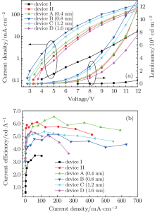
Figure 1(a) shows the J– V– L characteristics of OLEDs. It is obvious that the current density of device II is much higher than that of device I. Correspondingly, the luminance of device II is much higher than that of device I. The increase in current density for device II is ascribed to Cs2CO3 layer which can react with Al layer to form a small amount of Al– O– Cs complex to reduce the work function of the cathode.[7] At voltages below 11 V, the current density of the device A(0.4 nm) is slightly higher than that of device II because more Al– O– Cs complex is generated by inserting a 0.4-nm-thick Al layer into Cs2CO3 injection layer. However, at voltages above 11 V, the situation is reversed. This is probably because there are Cs atoms diffusing into Alq3 layer, resulting in enhancement of conductivity in device II. When a thin Al layer is inserted into thermally evaporated Cs2CO3 which decomposes into cesium oxides, [12] Al reacts with cesium oxides to form Al– O– Cs complex on the interface between Al and cesium oxides.[7] Though Al– O– Cs complex can reduce the function work of the cathode, the amount of Al– O– Cs complex is not enough because the thickness of the thin Al layer is only 0.4 nm. With the increment of the thickness of Al layer from 0.4 nm to 0.8 nm, the current density and luminance always increase, as shown in Fig. 1(a), and when the thickness of Al layer is 0.8 nm, the current density and luminance are the highest. However, the current density and luminance drop with further increase in the thickness of Al layer for device C (1.2 nm) and D (1.6 nm). This phenomenon can be explained by that when 0.8-nm-thick Al is inserted into Cs2CO3 injection layer, Al reacts with cesium oxides to form most Al– O– Cs complex. However, as the thickness of Al increases from 0.8 to 1.6 nm, Al cannot sufficiently react with cesium oxides so that there are some intrinsic Al on the interface.[7] As shown in Fig. 1(a), the variation of luminance of all devices is consistent with the variation of current density. The luminance of device B (0.8 nm) at the same voltage is always the highest due to the enhancement of electron injection. The luminance of device I, device II, device A (0.4 nm), and device B (0.8 nm) successively increases because more electrons are injected into EML to enhance the recombination rate of holes and electrons. For device C (1.2 nm) and device D (1.6 nm), their luminance is relatively low owing to the decrease in the amount of electrons injected into EML. From Fig. 1(b), we can see that device A (0.4 nm) shows the highest current efficiency among the all devices. Despite device B (0.8 nm) has the highest current density and luminance, its current efficiency is lower than device II, device A (0.4 nm), and device C (1.2 nm). Moreover, Alq3 is an electron-transporting material, so many electrons injected into Alq3 EML can easily lead to hole-electron unbalance.
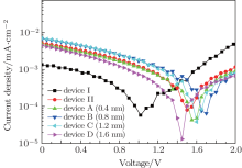
In order to reveal the work function of the cathodes Cs2CO3 (0.5 nm)/Al (x nm)/Cs2CO3 (0.5 nm)/Al (120 nm), and Cs2CO3 (1 nm)/Al (120 nm) in the devices, the devices are subjected to photovoltaic measurements conducted by a Keithly model 2400 power source under illumination of a Newport Oriel 150 W solar simulator (AM 1.5 G, 100 MW/cm2). The open-circuit voltage (Voc) obtained from photovoltaic measurement can reflect the built-in potential in the devices.[8, 13] Except for the cathode, all parameters are the same in the devices, so different Voc can reveal different work function of the cathode. The curves of the photovoltaic measurements for all devices are shown in Fig. 2. The Voc of all devices are 1.020097, 1.500635, 1.5503, 1.700229, 1.600405, and 1.44976 V, respectively. The Voc of device B (0.8 nm) is 1.700229 V, which is the highest in all devices. This means that the lowest work function of cathode can be obtained for device B (0.8 nm). The shift of all curves of photovoltaic measurements for different devices is consistent with the change of current density of different devices. Thus, it can be seen that inserting Al layer into Cs2CO3 to adjust the amount of Al– O– Cs complex can further reduce the work function of the cathode and lower electron injection barrier to enhance electron injection.
 | Fig. 2. Curves of photovoltaic measurements of device I, device II, device A (0.4 nm), device B (0.8 nm), device C (1.2 nm), and device D (1.6 nm). |
In addition, to further reveal the work function of the cathodes Cs2CO3 (0.5 nm)/Al (x nm)/Cs2CO3 (0.5 nm)/Al (120 nm) and Cs2CO3 (1 nm)/Al (120 nm), the configurations of Cs2CO3 (0.5 nm)/Al(x nm)/Cs2CO3 (0.5 nm)/Al (120 nm)/glass and Cs2CO3 (1 nm)/Al (120 nm)/glass are fabricated and their work function is measured by Kelvin probe. The wok function of Al is 4.2798 eV through measurement. For the configuration of Cs2CO3 (1 nm)/Al (120 nm)/glass, the work function is 3.7331 eV. For the configurations of Cs2CO3 (0.5 nm)/Al (x nm)/Cs2CO3 (0.5 nm)/Al (120 nm)/glass in which x is 0.4, 0.8, 1.2, and 1.6, the values of work function are 3.7210, 3.6423, 3.6665, and 3.7547 eV, respectively. We can find that the results of Kelvin probe measurements are in agreement with the results of photovoltaic measurements. Among these configurations, the lowest work function is obtained when the thickness of the thin Al layer is 0.8 nm. The Kelvin probe measurements provide the solid evidence for inserting a thin Al layer into Cs2CO3 injection layer to lower the electron injection barrier.
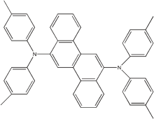
To validate the universality of this approach and expand its scope of application, we also construct another group of devices with a blue material DNCA (a derivation of N6, N6, N12, N12-tetrap-tolylchrysene-6, 12-diamine) as an emitting layer. Figure 3 shows the molecular structure of DNCA. The configurations of the devices are as follows: ITO/NPB (40 nm)/DNCA (30 nm)/Bphen (20 nm)/Cs2CO3 (0.5 nm)/Al (0.8 nm)/Cs2CO3 (0.5 nm)/Al (120 nm) and ITO/NPB (40 nm)/DNCA (30 nm)/Bphen (20 nm)/Cs2CO3 (1 nm)/Al (120 nm). Figure 4 shows schematic illustration of energy level diagram of the devices. It can be seen from Figs. 5(a) and 5(b) that the device with Al inserted into Cs2CO3 layer exhibits higher current density, luminance, and current efficiency compared to the device without Al layer inserted into Cs2CO3 layer. Especially, the performances of current density and luminance are similar to the devices based on Alq3, but the performance on current efficiency is reversed. This can be due to the fact that inserting Al layer into Cs2CO3 layer leads to more electrons injected from cathode and makes hole– electron pairs more balanced, given DNCA is a hole-transporting emitting material.[14]
 | Fig. 4. Schematic illustration of energy level diagram of the devices based on DNCA with and without a thin Al layer. |
In summary, we demonstrate a simple and effective method of inserting a thin Al layer into Cs2CO3 injection layer to improve the performance of the devices. We can control the amount of the Al– O– Cs complex by adjusting the thickness of the thin Al layer to lower the electron injection barrier and further enhance electron injection. For the devices based on an electron-transporting material Alq3, the maximal current efficiency (6.5 cd/A) can be achieved when the thickness of the thin Al layer is optimized to 0.4 nm. The photovoltaic measurements and Kelvin probe measurements indicate that the cathode can achieve the lowest work function when 0.8-nm Al layer is inserted into Cs2CO3 layer. To validate the universality of the approach, we fabricate another two devices based on a hole-transporting material DNCA, and the device with 0.8-nm Al layer inserted into Cs2CO3 layer shows better current density, luminance, and current efficiency compared to the device without Al layer inserted into Cs2CO3 layer. The maximal current efficiency increases from 4.51 cd/A to 4.84 cd/A.
| 1 |
|
| 2 |
|
| 3 |
|
| 4 |
|
| 5 |
|
| 6 |
|
| 7 |
|
| 8 |
|
| 9 |
|
| 10 |
|
| 11 |
|
| 12 |
|
| 13 |
|
| 14 |
|


