Cao Ya-Peng, Hu Yu-Feng, Li Jian-Tao, Ye Hai-Hang, Lü Long-Feng, Ning Yu, Lu Qi-Peng, Tang Ai-Wei, Lou Zhi-Dong, Hou Yan-Bing, Teng Feng. Electrical bistable devices using composites of zinc sulfide nanoparticles and poly-(N-vinylcarbazole)* . Chinese Physics B, 2015, 24(3): 037201
Permissions
Electrical bistable devices using composites of zinc sulfide nanoparticles and poly-(N-vinylcarbazole)*
Cao Ya-Penga), Hu Yu-Fenga)†, Li Jian-Taoa), Ye Hai-Hangb), Lü Long-Fenga), Ning Yua), Lu Qi-Penga), Tang Ai-Weib), Lou Zhi-Donga), Hou Yan-Binga), Teng Fenga)‡
Key Laboratory of Luminescence and Optical Information, Ministry of Education; Institute of Optoelectronic Technology, Beijing Jiaotong University, Beijing 100044, China
Department of Chemistry, School of Science, Beijing Jiaotong University, Beijing 100044, China
*Project supported by the National Natural Science Foundation of China (Grant No. 61377028), the Natural Science Funds for Distinguished Young Scholar, China (Grant No. 61125505), and the Fundamental Research Funds for the Central Universities, China (Grant No. 2014JBZ009).
Abstract
N-dodecanethiol capped zinc sulfide (ZnS) nanocrystals were synthesized by the one-pot approach and blended with poly (N-vinylcarbazole) (PVK) to fabricate electrical bistable devices. The corresponding devices did exhibit electrical bistability and negative differential resistance (NDR) effects. A large ON/OFF current ratio of 104 at negative voltages was obtained by applying different amplitudes of sweeping voltage. The observed conductance switching and the negative differential resistance are attributed to the electric-field-induced charge transfer between the nanocrystals and the polymer, and the charge trapping/detrapping in the nanocrystals.
Nanocomposites containing organic and inorganic nanomaterials have been extensively studied for their potential applications in nonvolatile memory devices.[1– 3] These nonvolatile memory devices utilize two conducting states (high or low) and are also called electrical bistable devices. So far, a large variety of nanomaterials, such as metal and inorganic nanoparticles (NPs), have been synthesized and explored for electrical bistable devices.[4– 8] Electrical bistable states have been successfully demonstrated in the solution-processed blend film of AgS, ZnO, or CdSe/ZnS nanoparticles with organics.[9– 12] However, the organics used in those works were mainly insulated polymers and nanocrystals used were typically toxic and hard to synthesize, which largely limit the further applications of these devices. On the other hand, ZnS nanocrystals are less toxic, easy to acquire, but rarely used in organic electrical bistable devices.
In this paper, N-dodecanethiol capped ZnS nanocrystals were synthesized by the one-pot approach and used to fabricate bistable devices with an indium-tin oxide/ poly(3, 4-ethylenedioxythiophene):poly-(styrene-sulfonate)/PVK:ZnS NPs/aluminum (ITO/PEDOT:PSS/ZnS:PVK/Al) structure at different concentrations of PVK: ZnS NPs. The corresponding devices successfully demonstrated bistable properties, with the maximum ON/OFF current ratio on the order of 104. The negative differential resistance effects were observed in the negative voltage region and attributed to the charge trapping/detrapping process in the nanocrystals.
2. Experiment
The ZnS colloidal nanoparticles capped by n-dodecanethiol used in this study were synthesized according to our previous report.[13, 14] 3 mmol zinc acetylacetonate (Zn(acac)2), 5 mL n-dodecanethiol (DDT), and 15 mL 1-octadecene (ODE) were poured into a 50-mL three-neck flask, and then the N2 flow was piped in to degas the mixture under magnetic stirring for about 30 min. Afterwards, the mixture was gradually heated to 240 ° C and kept heating at this temperature for 4 h, and then it was moved away from the heating mantle and cooled to room temperature naturally. Finally, the mixture was centrifuged and dried in a vacuum to complete the synthesis.
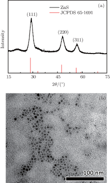
Figure 1(a) shows the X-ray powder diffraction pattern (XRD) of the as-obtained ZnS nanocrystals. It indicates that the resultant nanocrystals are orthorhombic chalcocite ZnS. The transmission electron microscopy (TEM) image of the as-obtained ZnS nanocrystals shown in Fig. 1(b) demonstrates that the nanocrystals have a spherical shape with a mean size of 8 nm.
Fig. 1. (a) XRD pattern of ZnS nanoparticles and standard diffraction lines of monoclinic ZnS. (b)TEM image of resultant ZnS nanoparticles.
The indium tin oxide (with a thickness of 100 nm and a sheet resistance of 15 Ω /◻ ) coated glasses were ultrasonically cleaned in deionized water, acetone, and isopropanol successively. The substrates were then dried by N2 and treated with UV ozone for 10 min. A thin PEDOT:PSS film was spin coated on the top of the ITO substrates at room temperature, and annealed at 150 ° C for 15 min to improve the device stability by hindering oxygen and indium diffusion through the anode. The poly-(N-vinylcarbazole) (PVK) and ZnS nanocrystals were mixed and dissolved in chlorobenzene solution with three mass ratios (1:1, 1:3, and 3:1), and then spin coated on the top of the PEDOT:PSS layer at 2000 rpm for 40 s in a glove box to form the active layer. Finally, 100 nm of Al was deposited on the ZnS:PVK layer by the thermal evaporation technique to complete the device fabrication under a vacuum of about 1 × 10− 6 torr. The cross-sectional area of the device is 4.5 mm2. Figure 2 shows the schematic diagram of the device and the chemical structures of PVK and ZnS. The current– voltage characteristics of the devices were tested by using a Keithley 2612 source meter controlled by a computer (Test Script Builder) at room temperature.
Fig. 2. Schematic illustration of the ITO/PEDOT:PSS/ZnS:PVK/Al organic bistable device and the chemical structures of PVK and n-dodecanethiol coated ZnS nanoparticle.
3. Results and discussion
The I– V characteristics of the devices are shown in Fig. 3. The voltage bias was cycled between − 5 V and 5 V starting from 0 V. The device based on pure PVK exhibits a small hysteresis, while a large electrical hysteresis loop can be observed in the device with ZnS nanoparticles. This evidences the existence of electrical bistable behavior in the device with the ITO/PEDOT:PSS/ZnS:PVK/Al structure. In addition, we compared the I– V characteristics for the devices with different mass ratios of PVK: ZnS NPs (1:1, 1:3, and 3:1) (the result is not shown here). The devices show similar current hysteresis in the I– V curve. The device with the ratio of 1:1 exhibits a higher amplitude of the hysteresis and a bigger ON/OFF ratio at the same sweeping voltage compared to those of the other two devices. The low and high resistance states correspond to the relatively ON state and OFF state, respectively. Under a voltage bias below 1.8 V, the device is in the high resistance state (OFF state). Resistive switching occurs at about 1.8 V, above which the device becomes more conductive. The threshold voltage is typically called VON.[15] When the voltage gradually drops from 5 V to − 5 V, the electrical current remains in the ON state till VOFF is reached. The VOFF is typically defined as the voltage bias required for switching to the OFF state, which is − 1 V in this case. A negative differential resistance is observed in the negative bias, which is a result of the charge trapping either in nanoparticles or in the defect states formed at the interface between the metal electrode and the organic semiconductor.[16, 17] In addition, after 15 min UV-ozone treatment, the device does not exhibit the electrical bistable behavior any more (Fig. 3), which indicates that the n-dodecanethiol surfactant plays an important role in the electrical bistability of the device, since the UV-ozone irradiation can remove the n-dodecanethiol surfactant.[18] This implies that the presence of the insulating n-dodecanethiol layer can prevent the charge recombination after removal of the external electric field.[19]
Fig. 3. The current– voltage curves of the ZnS:PVK composite film, the pure PVK film, and the ZnS:PVK composite film after 15 min UV-ozone treatment. The arrow head shows the dirrection of the sweeping voltages.
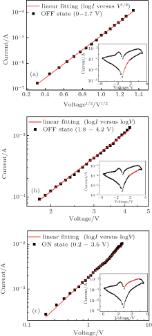
To clarify the carrier transport mechanism in our devices, we have fitted the experimental I– V curves in ON and OFF states using theoretical models on organic electronics. Figure 4 shows the experimental results and the linear fitting for the OFF state in the positive voltage region.
Fig. 4. Experimental results (open cycle) and theoretical linear fitting (solid line) of I– V characteristics in the positive voltage region. (a) Linear relationship of logI versus log V1/2 in the voltage range of 0– 1.7 V (OFF state). (b) Linear fit in double logarithmic scale in the voltage range of 1.8– 4.2 V (OFF state). (c) Linear fit in double logarithmic scale in the voltage range of 0.2– 3.6 V (ON state).
As shown in Fig. 4, the experimental I– V curve in the voltage range of 0– 1.7 V can be well fitted by the thermionic emission model (logI ∝ V1/2), indicative of the injection-limited current.[20] However, the log I– logV characteristics in the range from 1.8 V to 4.2 V (Fig. 4(b)) exhibit a large linear slope of 3.29, which is consistent with a trap-controlled space charge limit (TCLC) model (I ∝ Vα , α > 2).[21] The above fitting results suggest that charge carriers overcome the energy barrier at a voltage above VON and are captured by the traps in the ZnS nanospheres with an exponential distribution in the forbidden gap.
In contrast, the experimental I– V result in the ON state can be well described by an Ohmic model. In Fig. 4(c), a distinct linear relationship between logI and logV, with a slope of 1.27, is observed in the positive region (0.2– 3.6 V). The theoretical fitting indicates that the current in this region could be described by the Ohmic law (I ∝ V).[22] The results reveal that the traps in the ZnS nanospheres have been filled by the carriers during the aforementioned TCLC process. The trapped carriers boost the internal electrical field at the ZnS/PVK interface and change the device conductivity. All the theoretical fitting results are consistent with the charge trapping mechanism.
Based on the theory analysis above, the electrical bistability observed in our devices can be well explained by the field-assisted charge transfer between the ZnS nanocrystals and the PVK matrix. Under a positive voltage (0– 1.7 V), the injection of holes from the ITO into the highest occupied molecular orbital (HOMO) level of PVK occurs through the thermionic emission process and the holes existing at the HOMO level transport along the applied electric field direction through hopping among the PVK molecules. When the external electric field is high enough (1.8– 4.2 V), electrons on the HOMO of PVK may gain enough energy and tunnel through n-dodecanethiol into the ZnS nanoparticles, the charge transfer will occur between ZnS and PVK. As a result, the ZnS nanocrystals are negatively charged and PVK is positively charged, leading to an internal electric field. Therefore, the trapped charges in this process result in the transition of the device from OFF state to ON state. When the voltage is reduced from 5 V to 0 V, the negative charge on the nanoparticles may be stable due to the presence of the insulating n-dodecanethiol capping layer on the ZnS nanocrystals, which prevents the charge recombination after removing the external electric field. When a negative voltage is applied to the electrode (− 5– 0 V), because the holes captured in the ZnS nanoparticles under the negative electric field are released into the PVK matrix and then transported to the ITO substrate, the erasing process is performed.[15, 23– 26] The generated internal electric field disappears due to the release of the holes captured in the ZnS nanoparticles, which leads to the recovery of the device’ s resistance.
In summary, the working process of the device includes three stages. Firstly, the field-assisted charge transfer occurs between the PVK matrix and the ZnS nanoparticles when a high electric field is applied to the device. As a result, the resistance of the device decreases, representing a writing process. Secondly, when the voltage is reduced or removed, the conductivity of the device remains in the ON state with the help of the capping layer of the ZnS nanoparticles, which means the information is recorded in the device. At last, the charge can be released under a negative voltage so that the resistance increases, indicating an erasing process.
4. Conclusion
The nonvolatile memory devices with the structure of ITO/PEDOT:PSS/ZnS:PVK/Al were fabricated by a simple spin-coating method. The devices exhibited electrical bistability and negative differential resistance behavior due to the existence of the n-dodecanethiol coating the ZnS nanoparticles. The maximum ON/OFF current ratio of the device was as large as 104. The observed conductance switching and negative differential resistance can be attributed to the electric-field-induced charge trapping/detrapping at the interface between the nanocrystals and the PVK matrix.
In this paper, a WO 3 -based resistive random access memory device composed of a thin film of WO 3 sandwiched between a copper top and a platinum bottom electrodes is fabricated by electron beam evaporation at room temperature. The reproducible resistive switching, low power consumption, multilevel storage possibility, and good data retention characteristics demonstrate that the Cu/WO 3 /Pt memory device is very promising for future nonvolatile memory applications. The formation and rupture of localised conductive filaments is suggested to be responsible for the observed resistive switching behaviours.
a Institute of Microelectronics, School of Physical Science and Technology, Lanzhou University, Lanzhou 730000, China; b Institute of Microelectronics, School of Physical Science and Technology, Lanzhou University, Lanzhou 730000, China;Laboratory of Nano-Fabrication and Novel Devices Integrated Technology, Institute of Microelectronics, Chinese Academy of Sciences, Beijing; c Laboratory of Nano-Fabrication and Novel Devices Integrated Technology, Institute of Microelectronics, Chinese Academy of Sciences, Beijing 100029, China
In this paper, a WO 3 -based resistive random access memory device composed of a thin film of WO 3 sandwiched between a copper top and a platinum bottom electrodes is fabricated by electron beam evaporation at room temperature. The reproducible resistive switching, low power consumption, multilevel storage possibility, and good data retention characteristics demonstrate that the Cu/WO 3 /Pt memory device is very promising for future nonvolatile memory applications. The formation and rupture of localised conductive filaments is suggested to be responsible for the observed resistive switching behaviours.
1
2011
3.836
0.0
1
2010
3.794
0.0
... 8] Electrical bistable states have been successfully demonstrated in the solution-processed blend film of AgS, ZnO, or CdSe/ZnS nanoparticles with organics ...
1
2014
2.524
0.0
... [9#cod#x2013 ...
1
2014
3.836
0.0
1
2008
3.842
0.0
1
2010
3.794
0.0
... 12] However, the organics used in those works were mainly insulated polymers and nanocrystals used were typically toxic and hard to synthesize, which largely limit the further applications of these devices ...
1
2014
0.0
0.0
... [13,14] 3 mmol zinc acetylacetonate (Zn(acac)2), 5 mL n-dodecanethiol (DDT), and 15 mL 1-octadecene (ODE) were poured into a 50-mL three-neck flask, and then the N2 flow was piped in to degas the mixture under magnetic stirring for about 30 min ...
A facile one-pot heating process without any injection has been developed to synthesize different Cu-Zn-S-based nanocrystals. The composition of the products evolves from Cu(I)-doped ZnS (ZnS:Cu(I)) nanocrystals into heterostructured nanocrystals consisting of monoclinic Cu1.94S and wurtzite ZnS just by controlling the molar ratios of zinc acetylacetonate (Zn(acac)(2)) to copper acetylacetonate (Cu(acac)(2)) in the mixture of n-dodecanethiol (DDT) and 1-octadecene (ODE). Accompanying the composition transformation, the crystal phase of ZnS is changed from cubic zinc blende to hexagonal wurtzite. Depending on the synthetic parameters including the reaction time, temperature, and the feeding ratios of Zn/Cu precursors, the morphology of the as-obtained heterostructured nanocrystals can be controlled in the forms of taper-like, matchstick-like, tadpole-like, or rod-like. Interestingly, when the molar ratio of Cu(acac)(2) to Zn(acac)(2) is increased to 9:1, the crystal phase of the products is transformed from monoclinic Cu1.94S to the mixed phase composed of cubic Cu1.8S and tetragonal Cu1.81S as the reaction time is further prolonged. The crystal-phase transformation results in the morphological change from quasi-spherical to rice shape due to the incorporation of Zn ions into the Cu1.94S matrix. This method provides a simple but highly reproducible approach for synthesis of Cu(I)-doped nanocrystals and heterostructured nanocrystals, which are potentially useful in the fabrication of optoelectronic devices.
... [13,14] 3 mmol zinc acetylacetonate (Zn(acac)2), 5 mL n-dodecanethiol (DDT), and 15 mL 1-octadecene (ODE) were poured into a 50-mL three-neck flask, and then the N2 flow was piped in to degas the mixture under magnetic stirring for about 30 min ...
2
2009
3.794
0.0
... [15] When the voltage gradually drops from 5 V to #cod#x2212 ...
... [15,23#cod#x2013 ...
1
2006
1.921
0.0
... [16,17] In addition, after 15 min UV-ozone treatment, the device does not exhibit the electrical bistable behavior any more (Fig ...
Abstract The effect of voltage exceeding V min , the voltage corresponding to the local current minimum, on organic bistable devices is investigated. It is found that when the termination voltage V T exceeds V min , with the increasing V T , the bistable effect gets worse and finally lost at V T about 2 V min . However, the bistable effect can be recovered by applying a voltage pulse with amplitude near V min for milliseconds or longer. The existence of localized conducting micro-channels is suggested to account for the bistable effect.
... [16,17] In addition, after 15 min UV-ozone treatment, the device does not exhibit the electrical bistable behavior any more (Fig ...
1
2012
5.265
0.0
... [18] This implies that the presence of the insulating n-dodecanethiol layer can prevent the charge recombination after removal of the external electric field ...
1
2009
3.794
0.0
... [19] ...
1
1988
38.597
0.0
... [20] However, the log I#cod#x2013 ...
1
2002
0.71
0.0
... [21] The above fitting results suggest that charge carriers overcome the energy barrier at a voltage above VON and are captured by the traps in the ZnS nanospheres with an exponential distribution in the forbidden gap ...
1
2009
0.71
0.0
... [22] The results reveal that the traps in the ZnS nanospheres have been filled by the carriers during the aforementioned TCLC process ...
We have evaluated the effects of recombination processes in a chargestorage layer, either between trapped electrons and trapped holes orbetween trapped carriers and free carriers, on charge trappingmemory cell's performances by numerical simulation. Recombination isan indispensable mechanism in charge trapping memory. It helpscharge convert process between negative and positive charges in thecharge storage layer during charge trapping memoryprogramming/erasing operation. It can affect the speed ofprogramming and erasing operations.
a Institute of Microelectronics, Peking University, Beijing 100871, China; b Institute of Microelectronics, Peking University, Beijing 100871, China
We have evaluated the effects of recombination processes in a chargestorage layer, either between trapped electrons and trapped holes orbetween trapped carriers and free carriers, on charge trappingmemory cell's performances by numerical simulation. Recombination isan indispensable mechanism in charge trapping memory. It helpscharge convert process between negative and positive charges in thecharge storage layer during charge trapping memoryprogramming/erasing operation. It can affect the speed ofprogramming and erasing operations.
1
2012
1.148
1.2429
... 26] The generated internal electric field disappears due to the release of the holes captured in the ZnS nanoparticles, which leads to the recovery of the device#cod#x2019 ...
Electrical bistable devices using composites of zinc sulfide nanoparticles and poly-(N-vinylcarbazole)*
[Cao Ya-Penga), Hu Yu-Fenga)†, Li Jian-Taoa), Ye Hai-Hangb), Lü Long-Fenga), Ning Yua), Lu Qi-Penga), Tang Ai-Weib), Lou Zhi-Donga), Hou Yan-Binga), Teng Fenga)‡]


 , Li Jian-Tao