Synthesis and electrical properties of In2O3(ZnO) m superlattice nanobelt*
[Tang Xin-Yuea) , Gao Honga)†  , Wu Li-Li
b) , Wen Jinga) , Pan Si-Minga) , Liu Xina) , Zhang Xi-Tiana)‡ ]
, Wu Li-Li]
|
|


Corresponding author. E-mail: gaohong65cn@126.com
Corresponding author. E-mail: xtzhangzhang@hotmail.com
Project supported by the National Natural Science Foundation of China (Grant No. 51172058), the Key Project of the Science Technology and Research Project of Education Bureau, Heilongjiang Province, China (Grant No. 12521z012), and the Natural Science Foundation of Heilongjiang Province for Returned Chinese Scholars, China (Grant No. LC2013C17).
One-dimensional (1D) In2O3(ZnO) m superlattice nanobelts are synthesized by a chemical vapor deposition method. The formation of the In2O3(ZnO) m superlattice is verified by the high-resolution transmission electron microscopy images. The typical zigzag boundaries could be clearly observed. An additional peak at 614 cm−1 is found in the Raman spectrum, which may correspond to the superlattice structure. The study about the electrical transport properties reveals that the In2O3(ZnO) m nanobelts exhibit peculiar nonlinear I– V characteristics even under the Ohmic contact measurement condition, which are different from the Ohmic behaviors of the In-doped ZnO nanobelts. The photoelectrical measurements show the differences in the photocurrent property between them, and their transport mechanisms are also discussed.
Transparent conducting oxide materials, which have excellent performances in touch-sensitive or optoelectronic devices, have been widely studied.[1] In particular, alloys of indium zinc oxide have shown significantly enhanced electron conductivities and mobilities compared with zinc oxide. A homologous compound In2O3(ZnO)m (IZO) with a superlattice structure in thin film and that in bulk material could effectively be formed by ZnO doped with In up to a certain concentration.[2, 3] Furthermore, due to its fascinating electronic, optical, and magnetic properties, [4, 5] the synthesis of the one-dimensional (1D) semiconductor nanostructure has attracted a tremendous amount of attention in recent years. Zhang et al. have already synthesized IZO nanowires (NWs) with a modulated structure, analyzed the formation of such a superlattice in detail, [6] and even filled the gap in the JCPDS database.[7] Reports on photoluminescence (PL) properties, UV emission, and cathode luminescence emission[6, 8, 9] for these structures have also been published. Compared with NWs, nanobelts (NBs) each have a ribbon shape with a rectangular cross section and polar charges on top and bottom surfaces.[10] To superlattice structures, NWs grow along the [0001] orientation and form an axial superlattice, while the NBs grow in the 

The IZO NBs were synthesized by the conventional CVD method. Firstly, ZnO and In2O3 mixed powder in proper proportions as source materials were placed on an alumina boat, which was inserted into a horizontal tube furnace. The silicon substrates located in the downstream were coated with an Au thin film of 2 nm. The tube furnace was heated from room temperature to 1450 ° C and then kept for 20 minutes under a pressure of 3000 Pa. High-purity nitrogen flowed in continuously at a fixed flow rate of 100 sccm. After the furnace was naturally cooled down to room temperature, a layer of white product was obtained on the substrate. The synthesized products were characterized by scanning electron microscopy (SEM) (Hitachi, S-4800, Japan). The crystal structures of the samples were determined by x-ray diffraction (XRD) (D/MAX 2600/PC, Cu Kα radiation). The microstructure and chemical composition were investigated using a high-resolution transmission electron microscope (HRTEM) (Tecnai TF20, FEI, 200 kV) equipped with an energy dispersive x-ray (EDX) spectrometer. The Raman spectra for the samples were recorded using a micro-Raman system (JY-HR800, France) at room temperature, with a laser line of 514.5 nm used as the excitation source. In order to observe the layered superlattice structure of IZO NBs in detail by HRTEM, the sample was removed away from the substrate and embedded in resin. Then the superlattice NBs were cut into slices with a glass knife on an ultra-cutter (Leica EM UC7) after being dried.
To fabricate the individual IZO NB devices, the NBs were transferred from the grown substrate to a cleaned silicon substrate with a SiO2 layer on the upper surface. The electrodes at both ends of an individual ZnO:In NB were deposited using the microgrid template method[13] through the thermal evaporation.[14] The metal electrode consisted of Ti with a thickness of 80 nm and Au with a thickness of 100 nm.[15, 16] The distance between source and drain electrodes was about 20 μ m. Thereafter, the device was annealed at 450 ° C for 5 minutes in a high-purity N2 atmosphere to improve the contact between the individual NB and the electrode. The experimental results suggest that the annealing could significantly optimize the contact between NB and electrode. Finally, silver wires were connected with electrodes as guide wires. The relevant characteristics of I– V and the photoresponse were measured by a semiconductor parameter analyzer (Agilent, B1500A) at room temperature with a He– Cd laser line of 325 nm as the excitation source. Fluorescence dynamic curves were recorded by an optical spectrometer (Andor Shamrock SR-750) powered by a tunable Nd:YAG laser-pumped optical parametric oscillator laser.
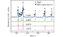
A series of samples with different doping levels are synthesized by the CVD method. The XRD pattern shown in Fig. 1 indicates the change of crystal composition with the increase of In doping concentration. The data of the concentrations came from the SEM measurements of sample substrates. As the doping level reaches and exceeds 4.98% , there appears a set of complex peaks. These peaks might relate to a superlattice structure, according to previous experience.[3, 7] Besides, when the doping level reaches a definite value, the superlattice structure might be formed in order to maintain the minimum system energy. Even so, determining the formation of the superlattice still needs further characterization, and the sample of 4.98% doping concentration (the mixture of 1.0-g ZnO and 0.2-g In2O3 powders is used as a precursor) is chosen as a typical representative.
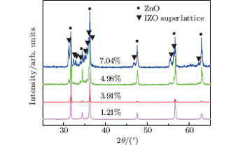 | Fig. 1. XRD patterns of the samples with different In doping concentrations. |
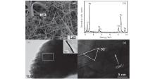
Figure 2(a) shows an SEM image of the as-synthesized products. On average, the length of the IZO NB is about tens of micrometres, and the width is hundreds of nanometers. The inset in Fig. 2(a) displays an enlarged SEM image. To obtain the detailed information about the composition of the sample, the EDX spectrum of an individual IZO NB from TEM measurement is investigated, which is shown in Fig. 2(b). The spectrometer analysis demonstrates the peaks of C, O, Zn, In, and Cu, while the signals of C and Cu are caused by the copper grid. As the IZO NBs are of planar superlattice structures, namely, the 

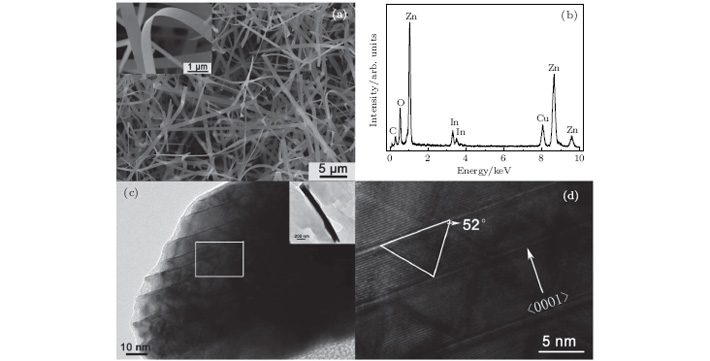 | Fig. 2. (a) SEM image of IZO NBs, with an inset showing a detailed SEM image of NBs. (b) EDX spectrum of an individual IZO NB from TEM measurement. (c) HRTEM of the slice cut from an IZO NB, with an inset showing a low-magnification TEM of the whole slice. (d) Enlarged HRTEM image of the marked area in Fig. 2(c). |
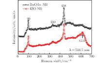
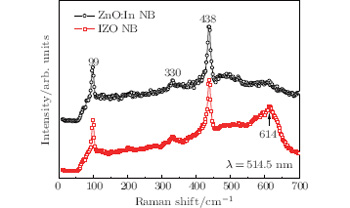 | Fig. 3. Raman spectra of IZO and ZnO:In NBs. |
To investigate the difference between the vibrate modes of IZO and ZnO:In NBs, the Raman spectra are measured as shown in Fig. 3. The peaks at about 99, 330, and 438 cm− 1 correspond to the E2L, E2H– E2L, and E2H phonon modes of the ZnO, respectively. An obvious difference could be observed in the spectrum of IZO NBs, and that additional peak at 614 cm− 1 is different from that of ZnO or In2O3.[19] This could be explained by the multiple-phonon scattering processes of the vibration mode, which is caused by the introduction of In ions.[20] However, it should be related to the formation of the IZO layered structure, not only the doping of In. A similar study, which attributes peaks around 621 cm− 1 in the Raman spectrum to the superlattice, has been reported.[12]
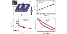
For characterizing the electrical properties of the IZO and ZnO:In NBs, the individual NBs are used to fabricate devices. The geometric sizes of the two NBs are similar, and the two kinds of devices are fabricated using the same method. The schematic diagram is shown in Fig. 4(a). A micro-grid template method is applied to evaporating electrodes. The inset shows the functional part of the device, which is an SEM image of an individual NB between Ti/Au electrodes. The I– V properties shown in Fig. 4(b) correspond to the two types of NBs, respectively. The curves are all measured in the dark environment at room temperature. The detailed information about these two types of NBs can be observed in Fig. 4(b). Under the low applied voltage in a range approximately from − 0.5 V to 0.5 V, the linear I– V characteristics for both the IZO and ZnO:In NBs indicate that the good Ohmic contacts between the NBs and Ti/Au electrodes are achieved. The two linear curves reveal a similar transport characteristic, and also suggest that they have similar conductivities. However, the curve of IZO NBs gradually deviates from linearity when the voltage reaches a certain value, which indicates that the transport behaviors of IZO and ZnO:In NBs are significantly different. This phenomenon shows that the increase of voltage can drive the electronic transport behavior of IZO NBs from the Ohmic regime to the space charge-limited (SCL) transport regime.[21] The current shows a power law dependence on the applied voltage, i.e., I ∝ Vβ .[21] The cross-over voltage of the SCL transport regime is a function of the free carrier concentration. The smaller the carrier concentration, the lower the voltage value will be. As an intrinsic semiconductor, the carrier concentration of IZO NBs is lower than that of ZnO:In NBs. Consequently, providing a low voltage, the IZO NBs transfer to SCL but ZnO:In NBs do not. As shown in Fig. 4(b), ZnO:In NBs still follow the Ohmic behavior in the whole applied voltage range due to their high carrier concentration. These results show that the electron mobility of IZO NBs is larger than that of ZnO:In NBs. Figure 4(c) shows time-dependent photoresponse properties of the IZO and ZnO:In NBs. The data are measured at a source voltage of 1.5 V. It can be seen that in the dark environment (the duration is 0 ∼ 20 s), the current values are similar to those in Fig. 4(b). While under illumination (the duration is 20 s∼ 60 s), the photocurrents are enhanced obviously. The photo-to-dark current ratio is defined as η = Iphoto/Idark, where Iphoto and Idark are the values of the photo current and dark current, respectively. It can be obtained from Fig. 4(c) that the η of IZO NBs is 1.6, and the value of ZnO:In NBs is 2.9. That is to say, the sensitivity of the IZO NB device is lower than that of the ZnO:In. Under UV illumination, the current value of ZnO:In NBs is higher than that of IZO NBs, because the number of trapping centers in ZnO:In NBs is bigger than that in IZO NBs due to their donor doping property.[22] In the energy-providing process, the trapped electrons obtained from the excited electrons can escape from the trapping centers and participate in the transport process, then lead to a high photocurrent value for ZnO:In NBs compared with that for IZO NBs. In the recovery process (the duration is 60 s∼ 260 s), the current of IZO NBs decays much faster than that of ZnO:In NBs. To explore the leading factor in the recovery process, the fluorescence dynamic curves of IZO and ZnO:In NBs are recorded as shown in Fig. 4(d). The decay curves could fit to an exponential decay function[23] with a parameter τ defined as a reset time until the value recovers to 1/e (37% ) of the maximum. The results give the relevant time constant τ of IZO NBs with a value of 251 ns, and the ZnO:In NBs with a value of 353 ns. It can be obtained that the decay time, i.e., the trapping center lifetime of IZO NBs, becomes shorter than ZnO:In NBs. In ions should act mainly as trapped electron centers in IZO NBs, but in ZnO:In NBs, the surface states play those roles. So, the difference between the two center types leads to the different lifetimes. This is consistent with the photo-generated carrier response phenomenon. Next, the recovery curves shown in Fig. 4(c) fit to an exponential decay function with two time parameters, which were defined as τ 1 and τ 2. The values of the parameters for ZnO:In NBs are τ 1Z = 3.2 s, and τ 2Z = 69 s, while for the IZO NBs τ 1I = 0.9 s, and τ 2I = 55 s. Normally, the photo-recovery phenomenon could be corresponding to a faster and a slower part, which could be related to the quick combinations of electron– hole pairs and the oxygen molecules adsorption, [14] respectively. The fast recovery time τ 1 for IZO NBs is less than that of ZnO:In NBs, which is consistent with the result that the lifetime of trapped electrons in IZO NBs is shorter than that in ZnO:In NBs, as shown in Fig. 4(d). The slow recovery process is attributed mainly to the surface states and the oxygen molecule adsorption. Because the geometric sizes of the two NBs are similar, there is only a little difference in slow recovery time τ 2 between these two structures.
 | Fig. 4. (a) Schematic diagram of the individual NB device, with an inset showing an SEM image of the NB between Ti/Au electrodes. (b) Dark I– V characteristics of IZO and ZnO:In NBs at room temperature. (c) Time-dependent photoresponses of IZO NB and ZnO:In NBs at a voltage of 1.5– V. (d) Emission lifetime measurements for IZO and ZnO:In NBs. |
In this paper, IZO NBs are synthesized by the CVD method. HRTEM patterns demonstrate the formation of IZO superlattice nanostructures, and zigzag boundaries can be clearly observed, which are found in planar superlattice nanostructures for the first time. An additional peak at 614 cm− 1 is found in Raman measurement, which may be related to the superlattice structure. The photoresponse phenomenon of IZO superlattice NBs is measured for the first time, and the results indicate that the photoelectric properties between IZO NBs and ZnO:In NBs are different. The nonlinear property of IZO NBs may be caused by the change of the transport mechanism. As an intrinsic semiconductor, the carrier concentration of IZO NBs is less than that of ZnO:In NBs, which could lead to a faster transfer to the SCL mechanism; and the number of trapping centers is also less than those of the doping materials, which may explain the difference in the photoresponse between the two NBs.
| 1 |
|
| 2 |
|
| 3 |
|
| 4 |
|
| 5 |
|
| 6 |
|
| 7 |
|
| 8 |
|
| 9 |
|
| 10 |
|
| 11 |
|
| 12 |
|
| 13 |
|
| 14 |
|
| 15 |
|
| 16 |
|
| 17 |
|
| 18 |
|
| 19 |
|
| 20 |
|
| 21 |
|
| 22 |
|
| 23 |
|