Breakdown mechanisms in AlGaN/GaN high electron mobility transistors with different GaN channel thickness values

Breakdown mechanisms in AlGaN/GaN high electron mobility transistors with different GaN channel thickness values |
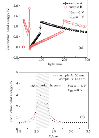
| Conduction band energy diagrams of devices with different channel thickness values (50 nm and 150 nm) (a) along the vertical cut-lines passing through the center of the gate and down through the buffer at V DS = 0 V and V GS = 0 V, and (b) along the horizontal cut-lines in the channel/ buffer interface, at V DS = 0 V and V GS = −6 V. |
 |