Corresponding author. E-mail: zhlmy@sina.com
Project supported by the Science and Technology Development Foundation of China (Grant Nos. 2012A0302015 and 2012B0302050).
Ternary metal chalcogenide semiconductor Ag8SnS6, which is an efficient photocatalyst under visible light radiation, is studied by plane-wave pseudopotential density functional theory. After geometry optimization, the electronic and optical properties are studied. A scissor operator value of 0.81 eV is introduced to overcome the underestimation of the calculation band gaps. The contribution of different bands is analyzed by virtue of total and partial density of states. Furthermore, in order to understand the optical properties of Ag8SnS6, the dielectric function, absorption coefficient, and refractive index are also performed in the energy range from 0 to 11 eV. The absorption spectrum indicates that Ag8SnS6 has a good absorbency in visible light area. Surface energies and work functions of
Organic pollutants are an important composition in dye wastewater. Nowadays, dyes have been widely used in textile industry, leather tanning industry, paper production, etc. Over one million tons of dyes are produced each year. How to degrade the dyes has become a worldwide problem.[1] In particular, the photocatalysis is a kind of potential technique for removing the hazardous organic contaminants from sewage. Accordingly, preparation of effective photocatalyts has been a hot topic.[2, 3] Most photocatalysts (such as TiO2, [4] ZnO, [5] and ZnS[6]) have catalysis only under ultraviolet (UV) radiation. However, almost 43% of the solar radiation energy is in visible light area (400– 750 nm), and only 4% comes from UV radiation.[7] Syntheses of photocatalyts, which have high catalytic activity under visible light radiation, are in pressing requirement.
Ag8SnS6 is a narrow band gap semiconductor, and its band energy gap is 1.39 eV.[8] Because its valence band contains S 3p orbital, it has good photocatalytic activity under visible light radiation. As reported in Ref. [9], Ag8SnS6 shows superior catalytic capability compared to commercial TiO2 under visible light radiation. The Eg of Ag8SnS6 was first reported by Osipishi in 1972, [8] and the structure was released by Wang in 1978.[10] The optical UV– vis absorption spectrum was measured by An et al.[9] Ag8SnS6 has a strong absorption spike in the visible region. However, to the best of our knowledge, there are no theoretical works to explain their electronic and optical properties. Hence, in order to obtain a further understanding of Ag8SnS6, theoretical investigation on the structural, electronic, and optical properties is necessary. In the present work, the electronic and optical properties, surface energies and work functions of Ag8SnS6 are investigated by performing the density functional theory (DFT) with generalized gradient approximation (GGA) and local density approximation (LDA).
All the calculations were performed within the density functional theory, using the plane-wave pseudopotential scheme. The generalized gradient approximation (GGA) with the Perdew– Burke– Ernzerhof (PBE) functional was used to treat the exchange-correlation effects.[11– 14] The electron function was expanded in the plane-wave basis set with a cutoff energy of 350 eV. Broyden– Fletcher– Goldfarb– Shanno (BFGS) scheme was used for k-point sampling in geometry optimization.[15] The Monkhorst– Pack k-points grid sampling was set at 2× 4× 2 points for the first Brillouin zone. The convergence tolerance parameters are set as follows: energy, less than 5.0 × 10− 6 eV/atom; maximum atoms force, less than 0.05 eV/Å ; maximum stress, less than 0.02 GPa; maximum displacement, less than 5.0 × 10− 4 Å . The Ag 4d105s1, Sn 5s25p2, and S 3s23p4 electrons were explicitly treated as valence electrons. In calculation of surface energies and work functions, the 


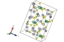
According to the literature, Ag8SnS6 belongs to Pna21 space group of the orthorhombic crystal system.[10] It contains four formula units in a single unit cell. There are two different types of S atoms in the Ag8SnS6 crystal structure. The first type connects Sn and Ag atoms together, and the other only form a bond with Ag atoms. The crystal structure of Ag8SnS6 is presented in Fig. 1. The equilibrium structural parameters were determined by using the Birch– Murnaghan equation.[22, 23] The Ag8SnS6 structure was optimized with the given parameters in Section 2. Experimental data are compared with geometry optimization results (see Table 1). Experimental[10] and calculated values of the lattice parameters match with each other very well. The optimized structure was used to calculate electronic and optical properties in the next section.
| Table 1. Experimental and calculated crystal structure parameters of Ag8SnS6. |
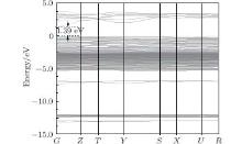
The band structure of Ag8SnS6 is shown in Fig. 2. Ag8SnS6 is a direct band gap semiconductor, and the conduction band minimum and the valence band maximum are at the G point. The band gap is about 0.58 eV, which is obviously less than the experimental value of 1.39 eV. The underestimated energy band gap values often come forth in the calculated simulation. This is related to the DFT limitations, and it does not take into account the discontinuity in the exchange– correlation potential.[24] For the sake of resolving this incongruity, the scissors operator is introduced.[15, 25] It can eliminate the difference between the experimental and calculated data, and shift the unoccupied conduction band with respect to the valence band. The scissors operator at 0.81 eV was performed in the present work. Table 2 shows band gap energies along with the valence to conduction band transition of Ag8SnS6. As we know, when the irradiation photon energy is greater than the semiconductor band gap, the electron will be excited to create an electron– hole pair. Photons exhibit a wavelike character with the wavelength (λ ), which is related to the photon energy Eλ by
 |
where h is Plank’ s constant, and c is the speed of light.[26] Therefore, in order to use visible light, the Eg of semiconductors should be below 3.0 eV (above 400 nm).[27] The narrower the energy band gap, the excited electrons and holes separate and migrate more easily. Because Ag8SnS6 has the narrow band gap of 1.39 eV, the electrons in the valence band of Ag8SnS6 are easily excited to the conduction band under visible light radiation. Consequently, Ag8SnS6 has excellent photocatalytic capability in the visible light area.
| Table 2. Symmetry of the valence to conduction band transition of Ag8SnS6. VB: valence band; CB: conduction band. |
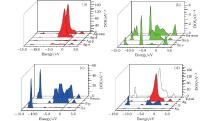
The partial and total density of states (PDOS and TDOS) can be used to analyze the composition of the energy bands. The DOS of Ag8SnS6 is presented in Fig. 3. The conduction band between 1.40 eV and 3.80 eV is contributed from Ag 5s and 5p states, Sn 5s and S 3p states, and these states are hybridized. The valence band is split into four sub-bands. In the uppermost valence band, Ag 4d, S 3p, and a small quantity of Sn 5p states are observed between 0 and – 5.40 eV. The second sub-band is contributed from Sn 5s and S 3p states, which is from – 6.80 eV to – 7.30 eV. The third one locates at 12.00– 12.40 eV, which consists of Ag 4d, Ag 5s, Ag 5p, Sn 5p, S 3s, and S 3p states. The lowest one is from – 12.70 eV to 13.00 eV. It is the main contribution of S 3s state, Sn 5s states, and Ag 4d, 5s, 5p states.
The charge density has been studied, and it was used to analyze the electronic structure of the system. The charge density distribution of Ag8SnS6 in (040) plane is displayed in Fig. 4. The covalent bond of materials can be associated with the sharing of the electrons between the atoms. As seen in Fig. 4, there is a distinct continuity in the constant charge contours among Ag, Sn, S atoms. The charge accumulations are presented between S and Ag, Sn atoms. These indicate that covalent bonds are formed between Ag and S atoms, Sn and S atoms.
The dielectric function is used to describe the optical properties of solid material. The dielectric constant ε is given by
 |
where ε 1 and ε 2 are the real and imaginary part of the dielectric function, respectively. The ε 2(ω ) can be used to describe the detail of the transitions between occupied and unoccupied electronic states, and the adsorptive behavior of materials. It is given by [15, 28]
 |
where u is the vector defining the polarization of the incident electric field, r is the electron’ s radius vector, e is the electric charge, 

 |
where P is the principal value of the integral, defined as
 |
The complex dielectric functions of different polarizations and polycrystalline are displayed in Fig. 5. Polycrystalline values are averaged over all polarization directions. The static dielectric constant ε 1(0) is 4.15 at zero frequency limit. Because there is negative scale from 3.97 eV to 9.15 eV, it indicates that the Ag8SnS6 has a metallic behavior in these energy zones. As seen from Fig. 5(b), there are five peaks which are marked by the symbols A (2.89 at 1.96), B (3.08 at 2.64), C (8.05 at 3.51), D (2.34 at 6.40), and E (1.38 at 7.02). The peak A is due to the electronic transition from S 3s (at – 6.90 eV) to Ag 5s (at – 4.96 eV), S 3p (at – 4.85 eV to – 2.89 eV), S 3p (at – 6.91 eV) to Ag 5s (at – 4.96 eV), Sn 5s (at – 4.96 eV) to Ag 5s (at – 6.90 eV) and Sn 5p (at – 4.81 eV) to Ag 4d (at – 2.89 eV). Peak B is contributed from Sn 5p (at – 4.36 eV) to Ag 5s (at – 1.89 eV). Peak C is mainly due to the transition from S 3p (at – 6.91 eV) to Ag 5p (at – 3.46 eV) and Sn 5s (at – 6.90 eV) to Ag 5p (at – 3.46 eV). Peak D originates from S 3p (at – 6.91 eV) to Ag 4d (at – 0.54 eV), S 3s (at – 6.90 eV) to S 3p (at – 0.47 eV), S 3s (at – 6.90 eV) to Ag 4d (at – 0.54 eV) and Sn 5s (at – 6.90 eV) to Ag 4d (at – 0.54 eV). Peak E may be due to transition from Sn 5p (at – 12.10 eV) to Ag 5s (at – 4.96 eV) and Ag 4d (at – 12.16 eV) to Ag 5p (at – 4.96 eV).
 | Fig. 5. Calculated dielectric function ε for Ag8SnS6 in different polarization and polycrystalline. (a) Real part ε 1(ω ); (b) imaginary part ε 2(ω ). |
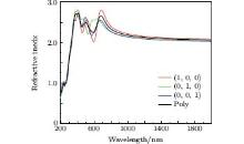
The refractive index n and Ag8SnS6 with different polarizations are presented in Fig. 6. The estimation of the refractive index is carried out by extracting square root of ε 1(ω ) in the limit of infinite wavelengths. The static refractive index n(0) of three polarizations are as follows: n(1, 0, 0) = 2.08, n(0, 1, 0) = 2.03, and n(0, 0, 1) = 2.00, the gap between them is very small. The trend of these curves are the same, all of them have 3 peaks from 400 nm to 700 nm. The maximum n of (1, 0, 0), (0, 1, 0), and (0, 0, 1) polarizations are 2.80 at 683 nm, 2.80 at 404 nm, and 2.74 at 407 nm, respectively. The n(0) of polycrystalline is 2.04, and the maximum n is 2.72 at 405 nm.
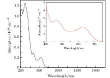
Ag8SnS6 is a significant photocatalyst, so the absorption coefficient is one of the most important parameters for measuring its catalytic activity. The calculated absorption spectrum of polycrystalline Ag8SnS6 is depicted in Fig. 7. It shows a wide absorbency from 190 nm to 750 nm, especially in the ultraviolet range (190– 400 nm), the absorption coefficient is almost above 8 × 104 cm− 1. It also shows a good adsorption in the visible light area (400– 750 nm), and the absorption coefficient locates at about 1 × 10⁴– 1.5 × 104 cm− 1. Comparison with the absorption spectrum of experiments in Ref. [9], the curves of these two spectrums have the same tendency in visible light area. However, the experimental data indicated that it has a weak absorption in the infrared region from 750 nm to 1350 nm. This difference might be related to the experiment conditions, the spectra were obtained by testing the nanocrystalline Ag8SnS6, while the calculation results were carried out by using the bulk Ag8SnS6. However, this evidence can explain that Ag8SnS6 has a marked catalysis activity under visible light radiation.
As seen in Fig. 8, the optical conductivity σ (ω ), loss function L(ω ), and reflectivity R(ω ) are displayed. Optical conductivity of a semiconductor is associated with the change in conductivity caused by illumination, either an increase or a decrease. Generally, the optical conductivity is the physical basis of optoelectronic applications of semiconductors. It contains the absorptive σ 1(ω ) (real part) and reactive σ 2(ω )(imaginary part) current response to a time-varying external electrical field of frequency. The optical conductivity σ (ω ) is displayed in Fig. 8(a). The real part of optical conductivity is zero when the energy is less than 1.46 eV and greater than 11.39 eV, and the peak is 3.52 fs− 1 at 3.60 eV. In the imaginary part, σ 2(ω ) value is zero at 7.56 eV.
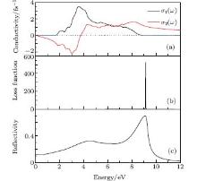 | Fig. 8. Optical spectrum of Ag8SnS6. (a) Optical conductivity. (b) Energy loss function. (c) Reflectivity. |
The loss function is a significance parameter describing the energy lost by an electron passing through a homogeneous dielectric material. The peak of loss function spectrum relates to the plasma resonance, and the corresponding frequency is called plasma frequency ω p. Figure 8(b) shows that the resonant energy locates at 9.25 eV. The reflection coefficient can be obtained for the simple case of normal incidence onto a plane surface by matching both the electric and magnetic fields at the surface. Reflectivity R(ω ) is shown in Fig. 8(c). The R(0) is 11.5%, and the maximum reflectivity value is 66.10% at 9.08 eV. The Ag8SnS6 has a good reflective ability in the ultraviolet and visible light area (190– 750 nm). The small value of reflectivity as well as absorptivity in the infrared region indicates that Ag8SnS6 is transparent in this range.
The photocatalytic reactions occur at the surface of Ag8SnS6 nanocrystal. So the surface energy is an important factor to influence the photocatalytic activity. The surface energy is the energy required to create a new surface, and it is difficult to measure in the experiment. Generally, the surface energies are determined at the melting temperature. In the calculation, the surface energy γ can be calculated by taking the energy difference between the total energy of a slab and a bulk reference amount
 |
where Eslab and Ebulk are the total energies of slab and bulk per unit cell, respectively, n is the number of unit cells in slab, and A is the surface area.[31]
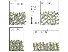
As seen from the literature, the nanocrystalline Ag8SnS6 have a submicropyramids structure, and its four outer faces correspond to 


| Table 3. Surface energies (J/m2) and work functions (eV) of Ag8SnS6 four different surfaces. |
The work function is the minimum energy required removing an electron from a solid to a point immediately outside the solid surface, or the energy needed to move an electron from the Fermi energy level into a vacuum. The expression is shown as follows:
 |
where Φ is work function, – e is the charge of an electron, ϕ is the electrostatic potential in the vacuum near the surface, and EF is the Fermi level inside the material.[32]
Usually, this energy depends on the orientation of the crystal; different orientation surfaces have different work function values. As we know, in the photocatalytic reaction, the first step is that electrons move outside from the Ag8SnS6 surface under the light radiation. The mechanism can be expressed as follows: Ag8SnS6 + hv → e– . Therefore, the work function is a significant parameter for estimating the catalytic activity of Ag8SnS6. Experimental and calculated work function values of Ag8SnS6 have not been reported yet. As seen from Table 3, GGA and LDA values were determined. The results of all four orientations were approximately at 4.5 eV. These values have little difference between each other. The 

Firstly, the structure of Ag8SnS6 is optimized, and the electronic and optical properties are calculated by performing the density functional theory (DFT) with the generalized gradient approximation (GGA). In order to eliminate the error of underestimation of calculation band gaps, a scissor operator of 0.81 eV is introduced. Dielectric function, absorption spectrum and refractive index are used to study the optical properties. Interestingly, the absorption spectra indicate that Ag8SnS6 has an excellent absorptivity in visible light area. The static refractive index n(0) of polycrystalline is 2.04. Next, surface energies and work functions of 


| 1 |
|
| 2 |
|
| 3 |
|
| 4 |
|
| 5 |
|
| 6 |
|
| 7 |
|
| 8 |
|
| 9 |
|
| 10 |
|
| 11 |
|
| 12 |
|
| 13 |
|
| 14 |
|
| 15 |
|
| 16 |
|
| 17 |
|
| 18 |
|
| 19 |
|
| 20 |
|
| 21 |
|
| 22 |
|
| 23 |
|
| 24 |
|
| 25 |
|
| 26 |
|
| 27 |
|
| 28 |
|
| 29 |
|
| 30 |
|
| 31 |
|
| 32 |
|


