Charge trapping in surface accumulation layer of heavily doped junctionless nanowire transistors

Charge trapping in surface accumulation layer of heavily doped junctionless nanowire transistors |
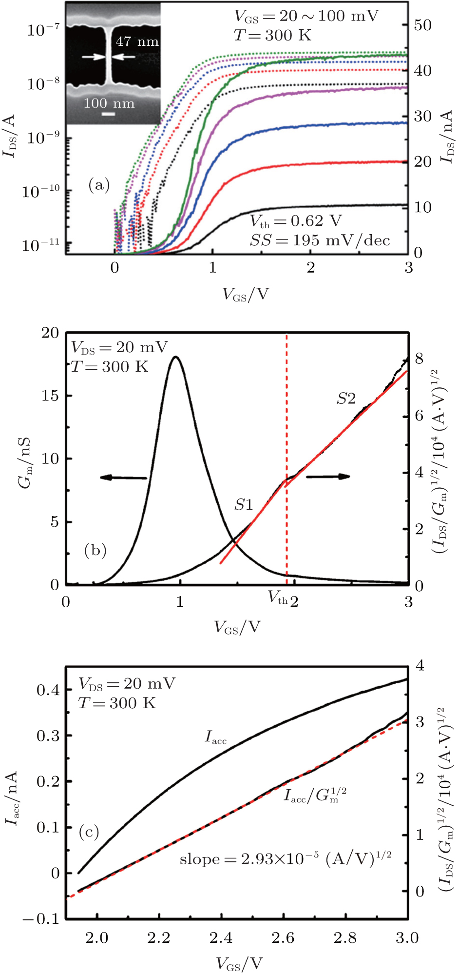
| Electrical performances of JNT measured at room temperature. (a) I DS– V GS curves for V DS values ranging from 20 mV to 100 mV in steps of 20 mV in both linear and logarithmic scale. The insert shows the SEM image of the nanowire after removing the SiO2 mask. (b) The transconductance G m as a function of V GS at V DS = 20 mV and the corresponding for the device. (c) The drain current of accumulation layer I acc and corresponding Y -function at V DS = 20 mV. |
 |