†Corresponding author. E-mail: qiluwei@ime.ac.cn
‡Corresponding author. E-mail: wangwenwu@ime.ac.cn
*Project supported by the National High Technology Research and Development Program of China (Grant No. SS2015AA010601) and the National Natural Science Foundation of China (Grant Nos. 61176091 and 61306129).
The positive bias temperature instability (PBTI) degradations of high- k/metal gate (HK/MG) nMOSFETs with thin TiN capping layers (1.4 nm and 2.4 nm) are systemically investigated. In this paper, the trap energy distribution in gate stack during PBTI stress is extracted by using ramped recovery stress, and the temperature dependences of PBTI (90 °C, 125 °C, 160 °C) are studied and activation energy ( Ea) values (0.13 eV and 0.15 eV) are extracted. Although the equivalent oxide thickness (EOT) values of two TiN thickness values are almost similar (0.85 nm and 0.87 nm), the 2.4-nm TiN one (thicker TiN capping layer) shows better PBTI reliability (13.41% at 0.9 V, 90 °C, 1000 s). This is due to the better interfacial layer/high- k (IL/HK) interface, and HK bulk states exhibited through extracting activation energy and trap energy distribution in the high- k layer.
As device dimensions shrink, high-k materials are being implemented by Si-CMOS technologies to alleviate the rapid gate current increase associated with aggressive oxide thickness scaling.[1] Owing to the continuous scaling of metal– oxide– semiconductor field-effect transistor (MOSFET), high-k gate dielectric materials are expected to replace traditional SiO2 in future complementary metal– oxide– semiconductor (CMOS) generation for low power circuits.[2] However, due to an extra interfacial layer and complicated band structure, [3] the reliability issues of CMOS devices with high-k/metal gate structure are becoming increasingly complicated and important, especially bias temperature instability (BTI).[4]
The TiN layer acts as a capping layer for high-k gate dielectric in the CMOS integration process. In particular, the positive bias temperature instability (PBTI) reliability of a device with TiN layer, as one of the major reliability issues, shows the dependence of the thickness of the TiN layer.[5] In this paper, the electrical characteristics and BTI degradations of high-k/metal gate MOSFETs with thin TiN capping layers (1.4 nm and 2.4 nm) are systemically studied. The PBTI differences and physical mechanisms are analyzed by extracting activation energy[6] and energy distribution of the trap in the high-k layer.
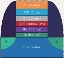
In this work, nMOSFETs were used as the test devices, which are shown in Fig. 1 with Hf-based dielectric stacks and different ultra-thin ALD TiN thickness values (1.4 nm and 2.4 nm). The equivalent oxide thickness (EOT) values of 1.4-nm TiN and 2.4-nm TiN were 0.85 nm and 0.87 nm, respectively. The gate width and length of transistor were 0.5 μ m and 0.5 μ m respectively. The test mode was the measurement-stress-measurement mode. The test was executed separately at constant temperatures of 60 ° C, 90 ° C, 125 ° C, and 160 ° C in a range of stress gate voltages (VG). The source and substrate were grounded.
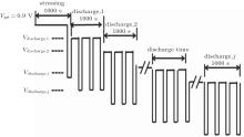
The nMOSFET was stressed at Vgstr = 0.9 V for 1000 s. After stress, Vg was changed to Vdischarge, 1 to start the discharge and the Vth shift against the “ discharge time” was monitored, as indicated in Fig. 2. Vdischarge ranges from 0.7 V to – 0.9 V in steps of 0.2 V and each Vdischarge lasted 1000 s.
The BTI of the MOSFET device induces the shifts of the device’ s parameters, such as Vth, GM, leakage current (Ig), etc.[7] A physical understanding of PBTI degradation mechanisms can be obtained through the variations of these electrical parameters, especially the Vth shift.
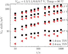
In Fig. 3, PBTI degradations versus time are shown for different ultra-thin TiN thickness values (1.4 nm and 2.4 nm) of high-k/metal gate nMOSFETs with gate-last process. The degradations of Vth with varying stress Vg directly show that the 2.4-nm TiN layer is better than the 1.4-nm layer. In other words, the 1.4-nm TiN layer has the worst PBTI: the Vt shift difference is 13.41% at 0.9 V, 90 ° C, 1000 s.
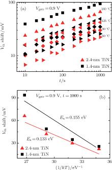
The temperature dependences of PBTI are shown in Fig. 4(a). The temperatures are 60 ° C, 90 ° C, 125 ° C, 160 ° C, and the voltage stress is 0.9 V. In Fig. 4(b), the extracted thermal activation energy (Ea) values are 0.133 eV and 0.155 eV, for samples with 2.4-nm TiN and 1.4-nm TiN layers, respectively. The activation energy of the 2.4-nm TiN layer is similar to that of the 1.4 nm layer. As is well known, the activation energy of high-k stack is around 0.03 eV– 0.04 eV, while that of conventional SiO2 gate is about 0.2 eV– 0.3 eV.[8, 9] It is demonstrated that the degradation mechanism[10] introduced by high-k material is dominant for both the 2.4-nm and 1.4-nm TiN layers.
Usually, the PBTI degradation occurs in high-k bulk.[11] In order to obtain the quantity and distribution of NOX in HK bulk, a new method is proposed, as described in Fig. 2, based on PBTI recovery characteristics.[12, 13] Figure 5(a) shows that the larger trap density of the device with thinner capping TiN under both 90 ° C and 160 ° C. Figure 5(b) shows the energy profile extraction for traps by using ramp recovery stress, which is described in detail below, [14] similar to that in our previous work.[15]
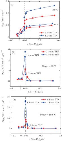 | Fig. 5. (a) Profiles of effective charge density (NOX) induced by PBTI recovery characteristics, (b) and (c) trap energy distributions at 90 ° C and 160 ° C, respectively. |
(i) Vth shift after completing discharge under each Vdischarge is converted into the effective charge density, i.e., NOX and plotted against Vdischarge, where NOX = Δ Vthɛ 0ɛ r/dq, with Δ Vth = Vth (end of each discharge)-Vth0 (Tstress = 0);
(ii) The next task is to convert Vdischarge into the energy level of EC, i.e., (ET − EC), by the oxide band structure, the same as that of our previous work, [15] where ET − EC = q· VOX and Vg = VOX + VS+ Vms, with ET being the trap energy level and EC the conduction band of substrate silicon, and VS the surface potential drop;
(iii) Plot NOX against (ET − EC) converted from the Vdischarge, as described in Fig. 4(a); and,
(iv) Obtain the differentiation of NOX against (ET − EC) as described in Fig. 5(a) and DOX against (ET − EC) as described in Figs. 5(b) and 5(c).
The results in Fig. 5 show that NOX(1.4 nm) > NOX(2.4 nm) and DOX(1.4 nm) > DOX(2.4 nm) for the cases of 90 ° C and 160 ° C. In particular, the maximum value appears at an energy 0.05 eV above the conduction band of silicon, which is shown in Fig. 6. This confirms that there are many more traps in the 1.4-nm TiN layer than in the 2.4-nm TiN layer. Figure 6 also shows the energy distribution of traps, indicating that there is a deeper trap in the HK bulk.
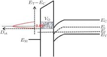 | Fig. 6. Band diagram of silicon/high-k/metal gate stacks. The shadow area represents the trap energy range that is strongly influenced by stress and the dot distribution is given. |
By combining the results, i.e., Ea = 0.13 eV for 2.4-nm TiN layer is closed to Ea = 0.15 eV for 1.4-nm TiN layer, in Fig. 4, as we just investigated, it is illustrated that trap generation happens in the HK dielectric layer, i.e., IL/HK interface and HK bulk.[16]
The influence of capping TiN thickness on PBTI could be explained by Nitrogen’ s out-diffusion from ALD TiN filling the oxygen vacancies in HK bulk, as described in Fig. 7.[17] In other words, the density of oxygen vacancies[18] is suppressed by thicker TiN capping layer due to the increased Nitrogen diffusion in the thicker (2.4 nm) film, which increases the stability of HK bulk and IL/HK interface.[19] So the thicker TiN capping layer shows better PBTI characteristics due to the better quality of the HK dielectric, as shown in Figs. 3 and 5.
The PBTI degradation of different thin TiN thickness with high-k/metal gate structure nMOSFETs is studied. Through a series of experiments, it is found that a thicker TiN capping layer shows better PBTI reliability due to the improvement of the IL/HK interface and HK bulk states by reducing the density of oxygen vacancies in HK gate dielectric through Nitrogen’ s out-diffusion from the TiN layer filling the oxygen vacancies in the HK bulk.
| 1 |
|
| 2 |
|
| 3 |
|
| 4 |
|
| 5 |
|
| 6 |
|
| 7 |
|
| 8 |
|
| 9 |
|
| 10 |
|
| 11 |
|
| 12 |
|
| 13 |
|
| 14 |
|
| 15 |
|
| 16 |
|
| 17 |
|
| 18 |
|
| 19 |
|


