†Corresponding author. E-mail: wangyue@hrbust.edu.cn
*Project supported by the National Natural Science Foundation of China (Grant No. 61201075), the Natural Science Foundation of Heilongjiang Province, China (Grant No. F2015039), the Young Scholar Project of Heilongjiang Provincial Education Bureau, China (Grant No. 1254G021), the China Postdoctoral Science Foundation (Grant No. 2012M511507), and the Science Funds for the Young Innovative Talents of Harbin University of Science and Technology, China (Grant No. 201302).
We propose an improved design and numerical study of an optimized tunable plasmonics artificial material resonator in the terahertz regime. We demonstrate that tunability can be realized with a transmission intensity as much as ∼61% in the lower frequency resonance, which is implemented through the effect of photoconductive switching under photoexcitation. In the higher frequency resonance, we show that spoof surface plasmons along the interface of metal/dielectric provide new types of electromagnetic resonances. Our approach opens up possibilities for the interface of metamaterial and plasmonics to be applied to optically tunable THz switching.
The field of metamaterial and plasmonics, combined with the unique electrical and optical properties of artificial metallic micro-/nano-structures, is one of the most attractive and profound area of photonics.[1– 3] Its rapid development has been driven by advanced micro/nano fabrication technologies, a powerful computational simulation tool, diagnostic systems, and sample appearance characterization, as well as by a number of important applications, such as improving the sensitivity of photodetectors, high sensitivity chemical sensing, and dynamic or tunable optical devices.[4, 5]
The progress of artificial electromagnetic metamaterials has led to the implementation of phenomena that do not occur in conventional natural materials, [6] which is particularly important for the THz frequency range because many natural materials inherently hardly respond to THz waves. The progression of THz science and technology depends on the realization of efficient components, such as adaptive lenses, filters, switches, modulators, dynamic polarization controllers, amplitude or phase modulators; however, the components that are needed to construct systems operating in the THz regime largely do not exist.
Metamaterials incorporated with semiconductors have led to the realization of a tunable dynamic function in a THz regime.[7– 9] Tunable metamaterials are employed at variable frequencies controlled by photo or electrical excitation within a quite wide frequency range instead of working at a fixed frequency that is only determined by their geometry.[10] Dynamic THz switches are complicated through photo-exciting free carriers in a semiconductor material, which shorts out the resonator gap; thereby, eliminating the electric resonance.[11, 12] Modulation of a THz wave with an applied voltage has been verified through a hybrid structure comprised of a planar metamaterial array and a Schottky diode. An applied voltage changes the conductivities of the semiconductor and graphene material at the capacitive split gaps and, therefore, is able to modulate the resonance strength of metamaterial devices.[13– 15]
In this paper, we consider periodic metallic metamaterial incorporated with photoconductor semiconductor in the gap on a thin dielectric film as an alternative structure to perform the tunable switching properties. The tunable functionality can be implemented with a transmission on the order of 61% in the lower frequency resonance, and it can be achieved by the effect of photoconductor-induced mode switching. There is a higher frequency resonance resulting from the generation of spoof surface plasmons polaritons (SPPs) along the interface between metal and dielectric.
The artificial metamaterial structure utilized in this study is based on a previously presented electric response split-ring resonator.[16] Although this structure has been widely studied, there are still some novel electromagnetic properties that need further study. This resonator strongly couples to a uniform electric field, in which the corresponding uniform magnetic field is neglected. Therefore, it can be regarded as an electric inductive– capacitive resonator. The geometrical dimensions are shown in Fig. 1(a). The planar unit cell array is fabricated on a flexible polyimide substrate with 16 μ m in thickness. The photoconductor silicon is located within the gap of the electric inductive– capacitive resonator in the unit cell. The electric inductive– capacitive resonator can be equivalent to a circuit, as shown in Fig. 1(b). This circuit includes an equivalent capacitor and two equivalent inductances, which provide capacitor (C) and inductance (L) for the circuit. The two equivalent inductances are connected to the capacitor in parallel. The electric field is coupled to the capacitor when the electric field is perpendicular to the gap, which causes the LC resonance that generates negative and positive electric polarizations along the resonance curve at different frequencies. Therefore, the resonator is either out-phase or in-phase, corresponding to the driving field. The resonant frequency of the equivalent circuit shown in Fig. 1(b) is ω 0 ∝ (LC)− 1/2.
 | Fig. 1. Schematic diagram of our designed metamaterial structure. (a) The structure of the unit cell. Metal and semiconductor are gold and silicon, respectively, the substrate material is polyimide. p = 36 μ m, a = 25.9 μ m, d = 10.8 μ m, g = 1.4 μ m, and w = 3 μ m. Both the gold and silicon are 200-nm thick. (b) Equivalent circuit of unit cell of Fig. 1(a), where R is the total equivalent resistance. (c) Top view of an array unit cell of designed metamaterial. |
The performance of the metamaterial device is characterized by numerical THz time-domain spectroscopy. All of the numerical simulation results are executed by using the CST Microwave StudioTM 2010 software tool. The appropriate boundary conditions are adopted for a unit cell, as shown in Fig. 1(a). These are similar to the actual conditions in a THz- TDS experiment, where the amplitude and phase of transmitted electric field are obtained for the electric inductive– capacitive resonator sample and the bare dielectric substrate (as a suitable reference). The complex transmission t(ω ) as a function of frequency can be obtained by dividing the Fourier intensity spectra of the sample and reference. Inversion of t(ω ) further permits model-independent calculation of the frequency-dependent complex permittivity ɛ (ω ). In the metamaterial, a lossy-metal model is used for gold, and its conductivity is σ gold = 4.09 × 10⁷ S/m. The dielectric substrate is regarded as a lossy polyimide with ɛ = 3.5 and a loss angular tangent of 0.003. We assume that the photo-excited layer is silicon with a thickness of 0.2 μ m. The frequency-dependent complex conductivity is given by

where ω p is plasma frequency, ɛ 0 is the permittivity of vacuum, Γ is the collision frequency, e is the free electron charge, m* is the effective carrier mass in Si, and N is the carrier density. The expression for ω p implies that the conductivity can be tuned through changing N. The dielectric constant ɛ (ω ) of Si is obtained, in terms of σ (ω ), from

where ɛ ∞ represents the frequency-independent optical dielectric constant of Si. In order to fit the resonance frequency in the case of no photo-excitation, we use ɛ ∞ = 11.9 and keep this value unchanged in the fitting procedure for all the cases. Notice that the carrier density of Si is taken to be 1.43 × 1010 cm− 3 without photo-excitation. Being more realistic, the upper limit of carrier density with N = 2.75 × 1018 cm− 3 is assumed, which is in agreement with the experimental results in Ref. [6].
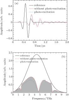
The time domain wave forms of the transmitted THz pulses through the metamaterial structure are shown in Fig. 2(a). From Fig. 2(a), it can be seen that the time-domain waveform for the reference substrate is represented by a single bipolar THz waveform. Adding a unit cell on the substrate, the oscillation of smaller amplitude appears on the transmitted THz waveform and an oscillation is moved from the initial bipolar pulse.
Figure 2(b) shows the corresponding Fourier-transform amplitude spectrum of the THz time-domain data. It is worth noting that there are two obvious spectral dips at 1.47 THz and 4.73 THz without photo-excitation. At a low frequency (1.47 THz), the dip is caused by the resonance absorption. It should be noticed, however, that there is a single dip at 4.73 THz with photo-excitation. At a frequency of 4.73 THz, the contribution of resonance transmission absorption depends on the interaction of the tailored metal surface with the THz pulse.
We first consider the metamaterial response without photo-excitation. The designed metamaterial structure is predicted to perform resonant behavior corresponding with the electric resonator. The transmission spectrum is shown in Fig. 3(a). The dashed line (red) denotes the response to the polarized direction of an electric field (E) perpendicular to the gap. It is seen that there are two definitely distinct resonances. In order to understand the mechanism of the f0 and fp resonances, a straightforward and intuitive method is proposed to analyze the distributions of surface current and electric field on the resonance frequencies. Figure 3(b) shows the current and field distributions for the case without photo-excitation. At f0 = 1.47 THz, the distribution of E strongly concentrates on the split gap. Associated with circulating currents in each metamaterial element, the LC response leads to the resonance at 1.47 THz, while the in-phase dipolar currents along the two sides (25.9 μ m lengths of the elements) of a unit cell in the metamaterial contribute to the resonance at fp = 4.73 THz. The spoof SPPs associated with large local electric field results in a significant increase of interaction strength between light and matter. Undoubtedly, the resonance mechanism of the two cases belongs to two distinct modes. In particular, a single broad absorption occurs at the resonance frequency of f∥ = 2.88 THz when the direction of E is parallel to the split gap. Compared with the resonance at fp, the broadening and redshift of the f∥ resonance is attributed to enhanced dipolar coupling, which results from two side elements (length a = 25.9 μ m) per unit cell. It is clear that no electric resonance is similar to the resonance frequency of f0 in this direction.
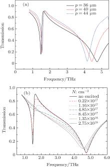
To better understand the nature of the fp resonance, we will present a further investigation of metamaterial with periods of 40 μ m and 44 μ m. A sub-wavelength unit cell on a substrate allows the electric field to penetrate the effective surface, which yields a bound surface wave (called spoof SPPs). The transmission spectra shown in Fig. 4(a) reveal that the resonance frequency fp depends on the periodicity of unit cell, which is in accordance with the explanation of spoof SPP excitations. In particular, there is almost no change at the f0 resonance frequency position. SPPs are transverse magnetic waves propagating along a metal/dielectric interface. The dispersion relation (frequency versus wave-vector, ksp) can be obtained by solving Maxwell’ s equations under the appropriate boundary conditions. The relation is[17]

where k0 = 2π f/c is a free space wave-vector, ɛ d and ɛ m are the dielectric permittivity and metal permittivity, respectively. At THz frequencies, | Re(ɛ m)| ≫ ɛ d and 
 | Fig. 4. (a) Transmission spectra in three different periods; (b) transmitted THz spectra as a function of frequencies in the case of different silicon carrier densities. |
Figure 4(b) reveals that the resonant transmitted THz spectra strongly depend on the carrier density of silicon. Without photo-excitation, there are two transmittance minima located at 1.47 THz and 4.73 THz corresponding to the transmittance values of 14% and 4%, respectively. There is a transmittance maximum at 1.6 THz with a transmittance of 91.5%. Between the two resonance frequencies (1.47 THz and 4.73 THz), the total transmittance decreases and the resonance of f0 initially weakens and its line-width broadens with increasing silicon carrier density (0.22× 1017 cm− 3– 4.85× 1017 cm− 3). As the carrier density of silicon further increases from 8.45× 1017 cm− 3 to 2.75× 1018 cm− 3, the resonance is continuously weakened and saturated at a transmittance of ∼ 75%. In this case, the resonator response does not show remarkable frequency dependence and is very weak near the resonance frequency of 1.47 THz, which happens because the silicon with higher carrier concentration shorts out the capacitive gap and it is difficult to establish the LC resonance. The results indicate the potential applications of an ELC resonator in a tunable narrowband THz switch. It is clear that the transmittance at f0 is strongly affected by silicon conductivity but the transmittance at fp is not significantly altered.
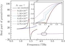
It is appropriate to describe the transmission properties of the proposed resonator in terms of equivalent dielectric constants. Such an approach is commonplace when studying plasmonic and metamaterial structures.[19, 20] The extracted dielectric constants are determined via inversion of the scattering parameters.[21] Figure 5 shows the corresponding equivalent permittivity around the electric inductive– capacitive resonance at various photoexcited carrier densities. Clearly, the equivalent permittivity ɛ ′ of the device is significantly turned by the photoexcited power. On the low frequency side of f0, the equivalent permittivity increases with frequency increment; however, it decreases to less than one and even becomes negative at higher frequencies near resonance frequency of f0. The sign change of ɛ ′ near f0, which is the frequency position of the transmission minimum, indicates that the structure is a form of electric resonator.[6, 7, 22] At fp, an electric resonant response in ɛ ′ is not observed, as shown in Fig. 5.
In this paper, we show that an ELC resonator with embedded photoconductor material can perform dynamic control at THz frequencies. Important transmission tunability (about 61%) at the resonance frequency f0 is observed, which demonstrates the possibility of an active narrowband THz switch under photo-excitation. In addition, we demonstrate the excitation of spoof SPPs in the metamaterial, which results in resonance at a high frequency of fp.
| 1 |
|
| 2 |
|
| 3 |
|
| 4 |
|
| 5 |
|
| 6 |
|
| 7 |
|
| 8 |
|
| 9 |
|
| 10 |
|
| 11 |
|
| 12 |
|
| 13 |
|
| 14 |
|
| 15 |
|
| 16 |
|
| 17 |
|
| 18 |
|
| 19 |
|
| 20 |
|
| 21 |
|
| 22 |
|


