


Effect of combined platinum and electron on the temperature dependence of forward voltage in fast recovery diode
[Jia Yun-Penga) , Zhao Bao†a)  , Yang Fei
b) , Wu Yua) , Zhou Xuana) , Li Zhea) , Tan Jiana) ]
, Yang Fei|
|


†Corresponding author. E-mail: summer201302@163.com
*Project supported by the Doctoral Fund of Ministry of Education of China (Grant No. 20111103120016) and the State Grid Corporation of China Program of Science and Technology, China (Grant No. 5455DW140003).
The temperature dependences of forward voltage drop ( VF) of the fast recovery diodes (FRDs) are remarkably influenced by different lifetime controlled treatments. In this paper the results of an experimental study are presented, which are the lifetime controls of platinum treatment, electron irradiation treatment, and the combined treatment of the above ones. Based on deep level transient spectroscopy (DLTS) measurements, a new level E6 ( EC-0.376 eV) is found in the combined lifetime treated (CLT) sample, which is different from the levels of the individual platinum and electron irradiation ones. Comparing the tested VF results of CLT samples with the others, the level E6 is responsible for the degradation of temperature dependence of the forward voltage drop in the FRD.
Platinum and electron irradiation introduce deep levels into the forbidden gap of silicon and are widely used as lifetime killing in fast recovery diodes (FRDs). In the past decades, deep levels associated with platinum and electron irradiation have been extensively studied. For platinum, although the exact location of the acceptor level is still open to question, most researchers have still located it between 0.2 eV and 0.3 eV below the conduction band. Experiments carried out in these laboratories showed an energy level of EC-0.23 eV.[1– 3] For electron irradiation, more than one level is introduced while two domination levels which are respectively close to the mid of band gap and the bottom of conduction band are supposed to influence carrier lifetime.[2]
Meanwhile, these deep levels can also result in different temperature dependences in VF among FRDs, which can significantly affect the ability to withstand the current surges and the roughness values of the high power circuits; however, a detailed study and analysis about it have not yet been made. In this work, the silicon diode samples are fabricated to introduce platinum, electron irradiation, and the combined impurities respectively. We show that the deep levels introduced by the above three methods have evident and different effects on the temperature dependence of VF. In the first part we discuss the deep level transient spectroscopy (DLTS) results of electron irradiation and combined impurities samples, giving evidence of a new deep level, i.e., E6 (EC-0.376 eV) existing in the combined samples. The second part is dedicated to the study of the I– V characteristics with platinum, electron irradiation and the combined impurities at different temperatures, and it can be revealed that the samples fabricated by electron irradiation and combined impurities possess the inverse performance of temperature dependence of VF, which should result from the effect of the new deep level E6.
The devices in this work are 1200 V/30 A TO-220 plastic-sealed p+ n− n+ diodes from Jilin Sino-Microelectronics Co., China. They have been fabricated on a lightly phosphorus-doped epitaxial silicon layer with a resistivity of 70 Ω · cm and a thickness of 100 μ m. This epitaxial layer was grown on a heavily doped n-type (n+ ) CZ substrate, 〈 111〉 oriented, with the resistivity in a range of 0.002 Ω · cm– 0.004 Ω · cm and a thickness of 500 μ m.
For platinum samples, platinum diffusions were carried out after the p+ boron diffusions, from a sputter-deposited 99.99% platinum film on the rear surface of substrates. The drive-in diffusions were carried out in dry nitrogen over a temperature range of 870 ° C– 900 ° C for 1 h. Then annealing was performed at 600 ° C for 20 min, eventually forming a stable U-shaped profile. In addition, some diode samples were irradiated at room temperature with 10-MeV energy at doses ranging from 30 kGy to 120 kGy using the electron linear accelerator. The experimental procedure for the combined lifetime control first formed stable platinum diffusion and then electron irradiation was performed. After high energy irradiation, all diodes were annealed at 300 ° C for 1 h to form stable defect levels.
After device fabrication was fully completed, the VF was measured using a Kelvin probe with 30-A forward current through the diode at different working temperatures. At the same time, DLTS measurements were made by using PhysTech FT-1030 for individual electron irradiation samples and the CLT samples. These two types of samples were measured under the same test conditions, which were the filling pulse bias (VP), the reverse bias (VR), the measurement period width (TW), and the filling pulse width (TP).
The forward voltage drop is a function of high level lifetime.[4] The high-level lifetime does not directly depend on the defect center position, but on trap concentration and capture coefficients.[5] The high-level lifetime (τ HL) formula is given by
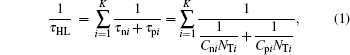
where Cni and Cpi are the capture coefficients for electrons and holes, respectively; τ pi and τ ni are the minority carrier lifetimes in heavily doped N-type and P-type silicon, respectively; and NTi is the defect density.
Nevertheless, recombination center parameters are different with the same lifetime control techniques, which are interfered by many factors such as semiconductor material, irradiation energy, annealing temperature and time. As indicated in a large number of papers, defect parameters induced by electron irradiation differ largely, which is mainly affected by irradiation energy.[6, 7]
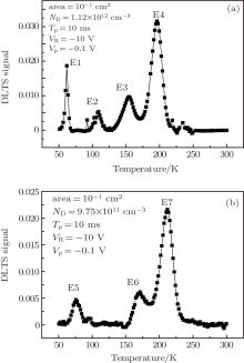
Figure 1 shows the majority carrier DLTS spectrum of the N-base of FRD after different lifetime control techniques. Seven levels E1– E7 are found in both types of the electron irradiated FRD and the CLT FRD. Based on the peaks in Fig. 1, through the Arrhenius system, all defect parameters including capture coefficients, energy position, and density are calculated as shown in Table 1. Comparing the peak values for the DLTS signal in Fig. 1(a), it is found that the vacancy oxygen (VO(− /0)) defect, double divacancy (V2(= /− )) defect, H-related (VOH(− /0)) defect, and single divacancy (V2(− /0)) defect are responsible for the electron irradiated peaks. The levels E1 and E4 have a dominant effect on the change of carrier lifetime. The peak E4 is the acceptor level of divacancy (V2(− /0)), which determines the high-level lifetime. The levels E2 and E3 each have a low concentration and capture coefficient and are annealed at relatively low temperatures, which have a negligible influence on the recombination activity.[8] According to Ref. [3], acceptor level (EC-0.23 eV) of platinum is an effective recombination level at high injection, while it acts as a weak recombination center at low injection.
 | Fig. 1. DLTS measurements of the N-base of FRD (a) after individual irradiation effects by electrons irradiation with a dose of 90 kGy and (b) after combined effects by electron irradiation with a dose of 90 kGy and platinum diffusion performed at 890 ° C for 1 h. |
| Table 1. Survey of deep levels identified in the N-base of irradiated diodes. |
Compared with DLTS signal peaks of individual electron irradiation, the levels E2 and E3 disappear in the DLTS signal of the CLT FRD. Meanwhile, platinum level (EC-0.23 eV) is not found and a new level E6 which belongs to neither the electron irradiation levels nor the platinum levels appears. Obviously, the level E6 is not a simply superposition with electron levels and platinum levels, but must be caused by combined effects.
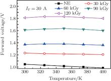
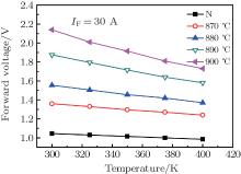
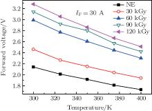
Lifetime-controlled samples show different temperature dependences of the forward voltage depending on the properties of induced defect.[2] Figure 2 shows the forward voltage dependences of the electron irradiated FRD on temperature, while figure 3 shows the measurements for platinum diffused FRDs. It is convinced that the temperature has a small influence on the VF of each of the electron irradiated samples. That is to say, at rated current, electron irradiated FRDs work at the positive or zero temperature coefficient, which is an advantage for paralleling applications. On the contrary, the VF of platinum diffused sample decreases with increasing temperature. This implies that FRD shows a negative temperature coefficient, which would stimulate the continuing current rise with the increasing of the temperature.
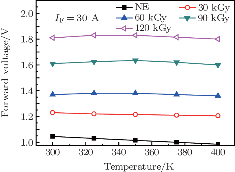 | Fig. 2. Temperature dependences of forward voltage drop for FRD after electron irradiation with different doses. |
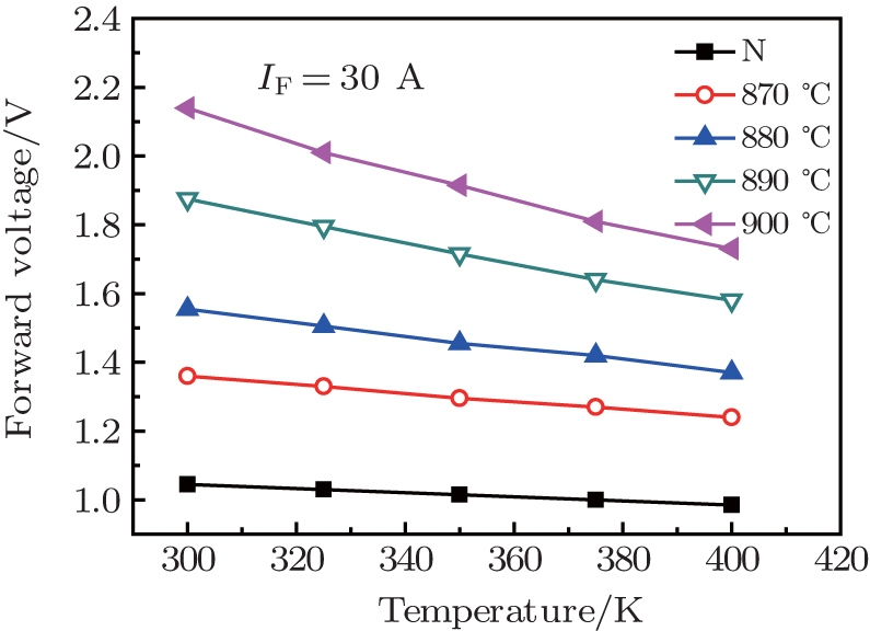 | Fig. 3. Temperature dependences of forward voltage drop for FRD after platinum diffusion at different temperatures for 1 h. |
Unlike the unirradiated FRDs, electron irradiation improves the temperature coefficients of the FRDs. The reason is that the concentration ratio between the E4 and E1 levels is very large (see Table 1). The level E4 is responsible for the carrier recombination in the lifetime at the high-level, that is deduced from the value of τ HL which is given by Eq. (1). Therefore, the forward voltage is strongly influenced by the temperature dependence of the capture coefficient of level E4. For platinum diffused samples, the forward voltage is mainly affected by the acceptor level (EC-0.23 eV), while the acceptor level has an inverse effect on the sample.
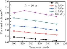
Figures 4 and 5 show the influences of the temperature on the forward voltage for the FRDs. Based on the results in Figs. 4 and 5, it is clear that with increasing temperature the forward voltage drop decreases. This is further supported by the change of the temperature coefficient as shown in Fig. 6. With the increase of electron irradiation dose, the Δ T/Δ T0 of the CLT sample increases negatively. This means that the CLT FRD irradiated by high energy electron cannot improve the temperature characteristic but aggravates it.
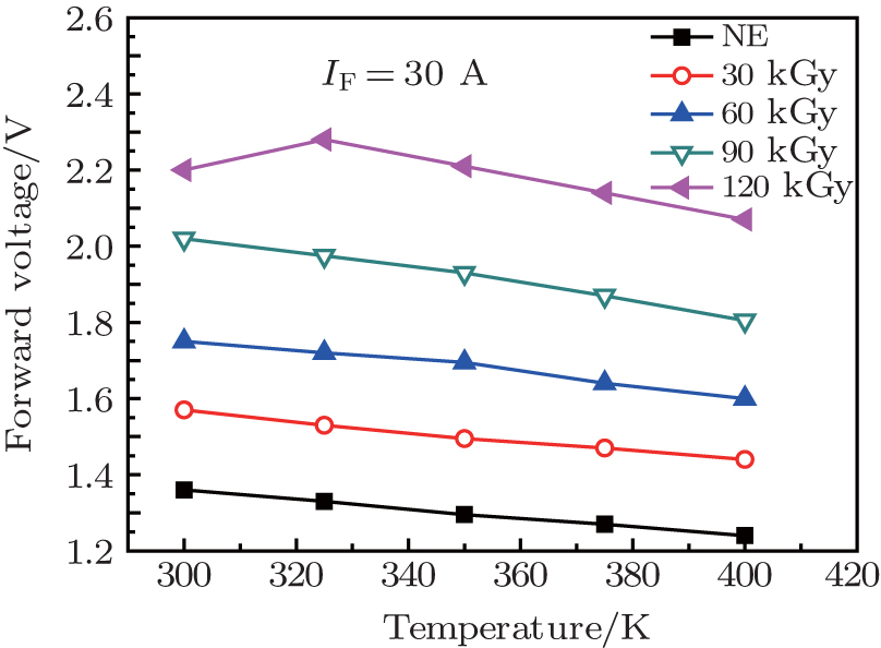 | Fig. 4. Temperature dependences of forward voltage for FRD after combined effects by platinum diffusion performed at 870 ° C for 1 h and electron irradiation with different doses. |
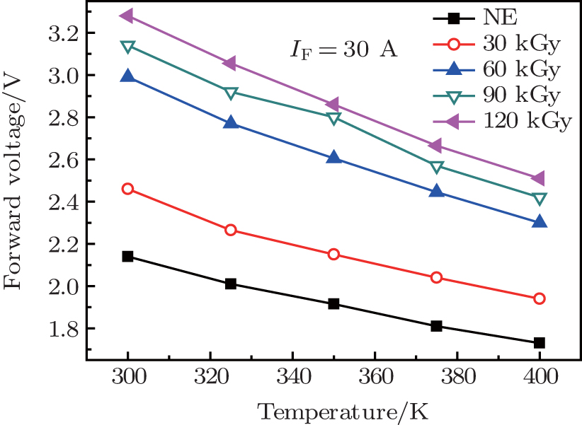 | Fig. 5. Temperature dependences of forward voltage for FRD after combined effects by platinum diffusion performed at 900 ° C for 1 h and electrons irradiation with different doses. |
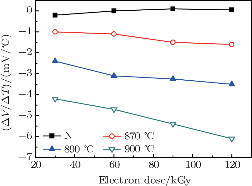 | Fig. 6. Temperature coefficients of forward voltage for FRD after combined effects by platinum diffusion and electron irradiation. |
In order to explain the intrinsic reasons of this phenomenon, we carry out the DLTS measurements for electron irradiated samples and the CLT samples. Based on analyses of the energy levels (see Fig. 1), it is demonstrated that there is an interaction between platinum and electron in the experimental process of combined lifetime, resulting in a change of recombination center data. It is worth pointing out that this kind of interaction produces a new level.
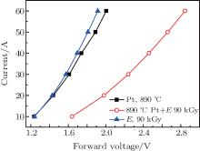
After DLTS measurements, the forward I– V characteristics on samples are shown in Fig. 7. It is clear that the voltage drop of the CLT FRD is higher than those of electron irradiated FRD and diffusion platinum FRD. As shown in Table 1, the capture rate and concentration of the level E5 are very small, so the level E5 gives little contribution to the high level lifetime of the CLT FRD. The E4 and E7 levels make similar contributions to the high level lifetime. According to the above analysis, the new level E6 must play such an important role in the high level lifetime that the CLT sample has a larger voltage. It is reasonable to make a conclusion that the level E6 is electrically active.
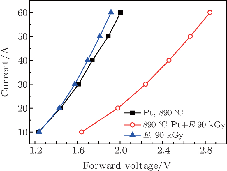 | Fig. 7. Forward I– V curves for the different lifetime controlled FRDs. |
The levels E6 and E7 make the main contributions to the forward voltage of the CLT FRD. Thus, the temperature dependences of the capture coefficient of the levels E6 and E7 determine the forward characteristics of the CLT FRDs. On the other hand, the levels E4 and E7 that are found to have the same position of the recombination center belong to the same defect. Therefore, the levels E7 and E4 have the same temperature dependence properties, which makes the FRD possess a positive temperature coefficient. However, the CLT FRD shows a negative temperature coefficient. It can be easily inferred that the temperature dependence of the level E6 is the most significant factor. Hence the level E6 dominates.
A combination of platinum diffusion and high energy electron irradiation is performed to study the temperature dependence of forward voltage for CLT FRD. Results show that the CLT FRD has a negative temperature coefficient of the forward voltage. Furthermore, it is found that there is a new level which makes devices possess negative temperature characteristics due to the interaction between platinum and electron.
| 1 |
|
| 2 |
|
| 3 |
|
| 4 |
|
| 5 |
|
| 6 |
|
| 7 |
|
| 8 |
|
| 9 |
|