

Design of ultra wideband microwave absorber effectual for objects of arbitrary shape
[Gong Yuan-Xun†a), b)  , Zhou Zhong-Xiang
a) , Jiang Jian-Tanga) , Zhao Hong-Jieb) ]
, Zhou Zhong-Xiang|
|


†Corresponding author. E-mail: gyxgyy@126.com
In this paper, we present the design of multilayer microwave absorbers comprised of CoFe alloy nano-particles and nano-flakes as fillers. The thickness of the unite layer is optimized by using the Genetic Algorithm. Efficient microwave absorptions over a wide frequency band and a range of incident angles are achieved by using multilayer absorbers. We show that the absorbers are effective not only for a planar surface but also for arbitrarily shaped objects as well.
As is well known, electromagnetic absorption (EMA) coating plays an important role in designing communication systems, including satellite and wireless systems, in which such absorbers are used to reduce electromagnetic interference and pollution.[1– 7] Typically, such EMA coatings are desired to have a specified level of absorption over wide incidence angles and ranges of the operating frequencies. Although a variety of monolayer EMA coatings with novel filler materials have been reported in the literature, few of these EMAs have achieved a sufficiently wide bandwidth that satisfies the requirements set forth in a wide variety of applications.[8– 11]
Because much more flexibility results from more tunable electromagnetic and structure parameters, the multilayer EMA absorber is believed to be more promising for wideband applications than the monolayer absorber.[12, 13] However, the design procedure for a multilayer absorber is complex, and the choice of the filler material is not straightforward. This is evidenced by the fact that there have been a large number of attempts to design multilayer EMAs by utilizing a variety of filler materials. The filler materials employed in most of the reported absorbers are dielectric, ferrite and ferromagnetic alloy materials, such as carbon nanotubes, ceramic fiber, barium ferrite, carbonyl fiber, etc., the permeability values of which are in a rather low level over the microwave band because of the limitation of Snoek’ s law and the eddy current effect. Owing to the low permeability values and comparatively high permittivity values, the impedance matching characteristics of these materials are poor and the dielectric loss is the single dissipation mechanism. Therefore a truly ultra-wideband performance has not yet been achieved in these absorbers. Benefiting from the progress of materials science, a ferromagnetic alloy nano-material with high microwave permeability values was successfully synthesized in our previous work, and exhibits a great potential as the candidate of filler materials to enlarge the operation bandwidth of multilayer absorber.[14, 15]
In addition, most of the reported multilayer absorbers are designed for the case of normal incidence, and the performance would deteriorate remarkably with the increase of incident angle. However, the absorber is required to possess stable performance against the varying of incident angle because of the complicated shape characteristics of practical objects. Furthermore, the reflection coefficient characteristic of the absorber backed with an infinite metal plane is traditionally adopted to evaluate the EMA performance. Whereas, the radar cross-section (RCS) reduction effect of the absorber backed with finite metal objects of plane-like, incline-like and camber-like shape should also be taken into account to make the performance evaluation more complete.
The objective of this work is to explore absorbers with ultra-wideband performance in both the cases of normal and oblique incidence. Since the number of parameters to be adjusted in designing the multilayer EMA can be quite large, computer optimization methods, such as the Genetic Algorithm (GA), are commonly adopted to solve the problems of designing multilayer absorbers.[16, 17] In the present work, an improved GA available for oblique incidence is used to design multilayer EMAs with ultra-wideband absorption characteristics over a wide range of incidence angle. A systematic procedure for designing multilayer EMAs is also included. And the RCS reduction effect of coating the absorber onto the surface of some objects with different shape characteristics is evaluated by using EM simulator GEMS.
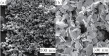
CoFe alloy nano-particles (NPs) and nano-flakes (NFs) are chosen to be the filler materials of the multilayer absorber. Figure 1 shows the scanning electron microscopy (SEM) images of CoFe alloy NPs and NFs. CoFe alloy NPs are sphere-like and about 100 nm in diameter, and CoFe alloy NFs are flake-like and about 500 nm in diameter.
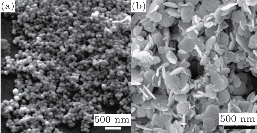 | Fig. 1. SEM images of (a) CoFe alloy nano-particles and (b) CoFe alloy nano-flakes. |
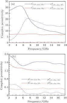
The electromagnetic properties of filler materials are measured by using a vector network analyzer (VNA, Agilent N5230A) in the transmission/reflection mode. 20 vol% filler materials and 80 vol% paraffin are mixed adequately and pressed into a mode to fabricate VNA specimens. The VNA specimens are coaxial torus with an inner diameter of 3 mm, outer diameter of 7 mm, and thickness values of 3 mm– 3.5 mm. Figure 2 shows the electromagnetic properties of CoFe alloy NPs and NFs. As indicated in the figure, the permeability values of these two filler materials remain at a rather high level over the frequency band of 2 GHz– 18 GHz. In particular, due to the unique plate-like morphology, both the real and imaginary part of the permittivity of NFs are several times higher than those of NPs. To take advantage of the distinct electromagnetic characteristic, the NPs and NFs are set to be the filler materials of the impedance matching layer and dissipation layer of the multilayer absorber, respectively.
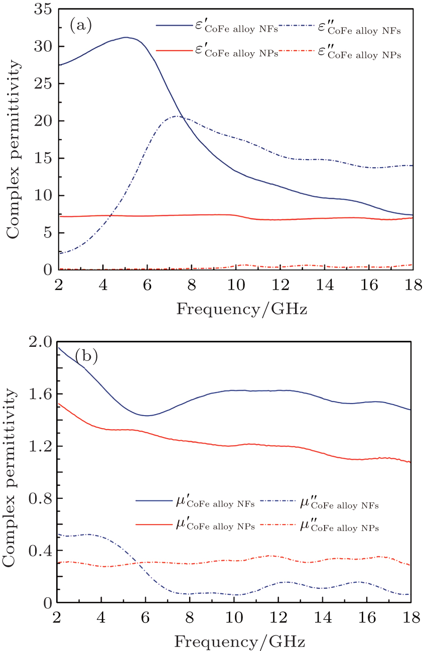 | Fig. 2. Complex permittivity and permeability spectra against the frequency of CoFe alloy nano-particles (NPs) and nano-flakes (NFs). |
Microwave absorbing performance of coating with different filler materials[18– 20] is presented in Table 1. As shown in the table, the dielectric loss of CoFe alloy NFs is 0.09– 1.87, which is rather higher than those of CoFe alloy NPs and the rest of listed filler materials. Moreover, the microwave absorbing performance in a frequency range of 4 GHz– 8 GHz of CoFe alloy NFs is remarkably superior to those CoFe alloy NPs and the rest of the listed filler materials.
| Table 1. Microwave absorbing performances of coatings with different filler materials. |
The multilayer EMA absorber is designed by the simple GA method, in which the reflection coefficient is calculated according to transmission line theory as reported in Ref. [21]. The thickness of each layer (di) is set as a parameter to be optimized. Since our aim is to design multilayer EMAs with a wide bandwidth, we choose the effective absorption bandwidth (BWeff) as a fitness function for the GA, in which the reflection coefficient is less than – 10 dB. The GA Toolbox of Matlab is employed to perform the optimization process. For a typical optimization procedure, the initial popular size is set to be 200, the mutation is set to be 0.15 and the crossover function is set as a scattering model. We run the optimization at least three times to ensure the stability of the design.
The performance of the EMAs in a function of the incidence angle and the RCS reduction effect of coating the absorber on the surface of perfect electrical conductor (PEC) objects with different shaped characteristics are evaluated by using the general-purpose EM simulator GEMs.
We begin with the simple case of a 2-layer absorber with NPs and NFs layers for the top and bottom layers. The optimized thickness values of these layers are found to be 1.25 mm and 1.75 mm, respectively. Figure 3 shows the reflection coefficients of the 2-layer absorber simulated by using GEMS, and their comparison with the reflection coefficients of the two monolayer absorbers containing either NPs or NFs as fillers. The total thickness of each of these three absorbers is 3 mm. As seen from the figure, an effective absorption performance of less than − 10 dB in the entire frequency band ranging from 4.6 GHz to 18 GHz is achieved in the 2-layer absorber, and this is obviously wider than the frequency range of the two monolayer absorbers with identical thickness. Moreover, the BWeff of 13.4 GHz is a much larger broadband than that of the reported absorber filled with low permeability material which is usually composed of 4 or 5 layers. For example, the operation bandwidth of the 4-layer absorber designed by Weile et al. covers the frequency band of 2 GHz– 8 GHz.[22] The BWeff of the 5-layer absorber designed by Michielssen et al. is 4.3 GHz.[23]
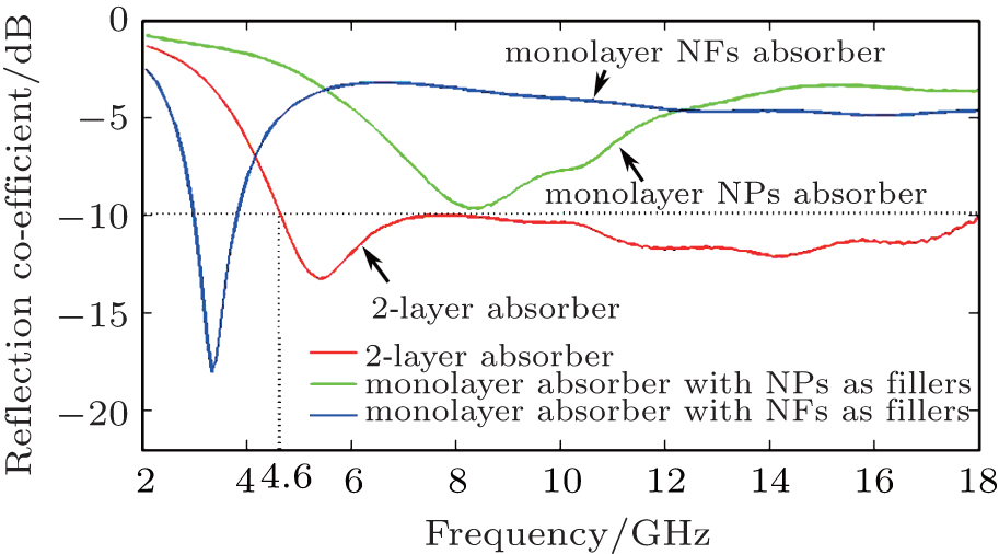 | Fig. 3. GEMS simulated reflection coefficients versus frequency of 2-layer and monolayer absorber containing either NPs or NFs as fillers. |
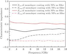
Generally, the performance of an absorber is determined by two factors. The first factor is the surface impedance, which determines how much energy of the incident EM wave can be transferred into the absorber. The surface impedance of a multilayer absorber is intimately related to the characteristic impedance (Z0) of the top layer. Figure 4 shows the variations of the Z0 with the frequency of monolayer coatings containing NPs and NFs as fillers, respectively. The real and imaginary parts of the Z0 of the coating utilizing NPs as the filler hover around 0.45 and 0.05 respectively in a frequency range of 4 GHz– 18 GHz, while the corresponding values are 0.25 and 0.1 for the coating with NFs serving as the filler. Since the real and imaginary parts of Z0 of the NPs layer is closer to those of free space, it is evident that its impedance matches to the free space much better than the case of NFs layer, which implies that less energy is reflected from the surface and more energy would be transferred into and dissipated inside the 2-layer absorber if we choose NPs for the top layer rather than NFs for the top layer.
 | Fig. 4. Characteristic impedance curves of monolayer coating containing NPs and NFs as filler. |
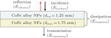
The second factor is the intrinsic dissipation efficiency of the filler material, which determines the efficiency of attenuation of the incident energy as an EM wave transfers through the absorber. The intrinsic dissipation efficiency of the filler material means the ratio of the energy dissipated inside the absorber to the incident energy. This quantity can be computed by using GEMS simulation for both the monolayer and 2-layer absorbers through removing the PEC backing, which is to eliminate the interference induced by multiple reflections from the surface of the PEC plate. Figure 5 illustrates the 2-layer absorber without PEC background.
 | Fig. 5. Illustration of 2-layer absorber without PEC background. |
The energy of the incident EM wave can be divided into three parts, namely reflection, transmission and dissipation. The intrinsic dissipation efficient denoted as Sdissipation can be calculated as follows:


where Eincidence, Ereflection, Etransmission, and Edissipation are the energies of incident, reflection, the transmission part, and dissipation part, respectively. S11 and S21 are the reflection coefficient and the transmission coefficient of the absorber, respectively.
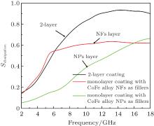
The simulated S-parameters as well as Sdissipation values of 2-layer and monolayer absorbers are deduced from Eqs. (1)– (3), and the variations of Sdissipation with frequency are shown in Fig. 6. We note from the figure that Sdissipation of the monolayer absorber with NFs as fillers increases from 0.14 to 0.62 in the frequency band of 2 GHz– 16 GHz, which is obviously higher than that of the monolayer absorber with NPs as fillers, whose value changes from 0.05 to 0.6. The reason for the higher Sdissipation of NFs’ layer can be ascribed to the higher imaginary part of permittivity as reported in our previous work, which leads to a higher dielectric loss tangent (tanδ ε ) and consequently higher dissipation capability. Moreover, the dissipation efficiency of the 2-layer absorber is obviously superior to those of the other two monolayer absorbers. Since the 2-layer absorber can be viewed as an NFs’ layer covered with an impedance matching layer (NPs’ layer) or as an NPs’ layer partly replaced by a dissipative layer (NFs’ layer), the higher Sdissipation of the 2-layer absorber attributed to a combination of improved surface impedance match and enhanced dissipation capability layer, both of which are helpful in improving the dissipation efficiency.
 | Fig. 6. Variations of Sdissipation with frequency of 2-layer and monolayer absorber containing NFs and NPs as fillers. |
As mentioned above, multilayer absorbers with the desired EMA performance should be composed of two functional parts. The top one should be the impedance matching layer, which should have an impedance close to that of free space to ensure as much as possible that the incident energy passes through the surface. The lower one should be the dissipation layer, which should possess high dissipation efficiency to attenuate the energy during the EM wave propagating through the absorber.
To further extend the effective absorption bandwidth, multilayer EMA absorbers with more than two layers are designed, and the details of coating structure are presented in Table 2. As indicated in this table, NPs’ and NFs’ layers are chosen to be the impedance matching layer and the dissipation layer, respectively, and the air gap is introduced to separate the NFs layer.
| Table 2. Thickness values and filler materials of each unit layer of GA designed multilayer absorber. |
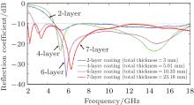
Figure 7 shows the simulated results obtained by using GEMS for the reflection coefficients of multilayer absorbers as we vary the number of layers. It is evident that increasing this number is helpful for the increase of BWeff. Particularly, the EMA performance in the lower frequency range is obviously improved and a reflection coefficient less than − 10 dB in the entire frequency band of 2 GHz– 18 GHz is achieved with a 7-layer absorber whose thickness is 23.18 mm. Moreover, three absorption peaks located around 2.2, 3.3, and 6.3 GHz are observed, and the minimum reflection coefficient is found to be – 36.4 dB.
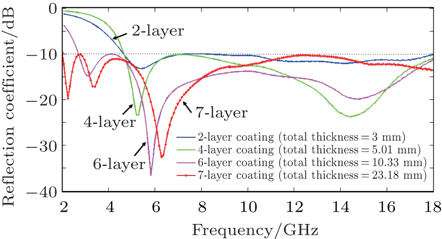 | Fig. 7. Curves of reflection coefficient versus frequency of multilayer absorber backed by a PEC plate for different numbers of layers. |
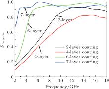
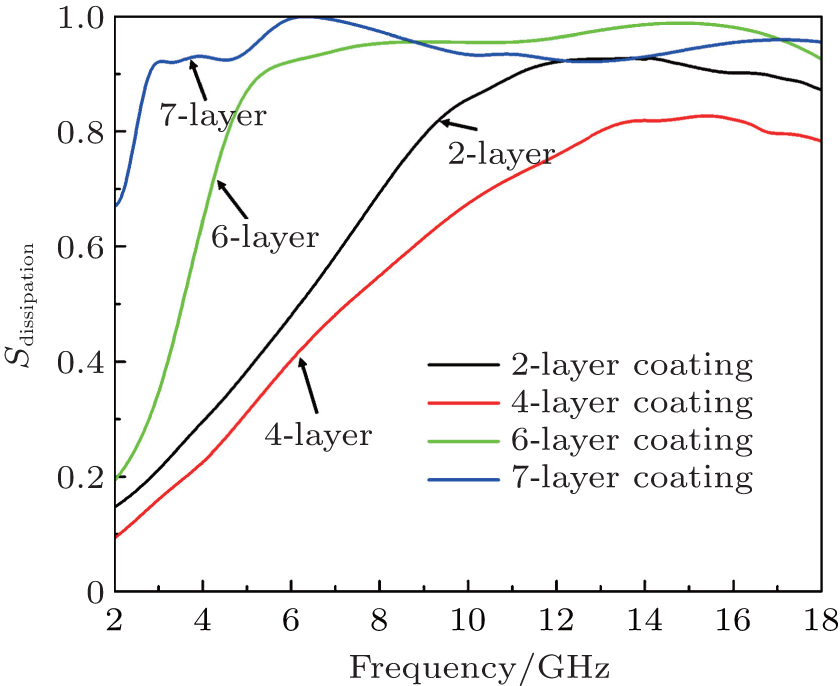
Figure 8 shows Sdissipation spectra of multilayer absorbers for different numbers of layers. As shown in the figure, the dissipation efficiency of the 7-layer absorber is maintained at a high level in the entire frequency band and is improved in the low frequency region. This, in turn, helps to provide the performance of the 7-layer absorber that has an ultra-wideband.
 | Fig. 8. Sdissipation– frequency curves of multilayer absorbers with different layer numbers. |
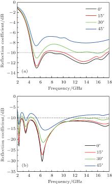
Since in a practical application the absorber may be used to coat an object of arbitrary shape, we need to design the absorber to provide good performance not only over a wide frequency band but also for a wide range of incident angles. To investigate the wide angle performance of the designed multilayer absorber, we simulate a 2-layer absorber and a 7-layer absorber each backed by a PEC plate for different incident angles, respectively. As shown in Fig. 9(a), the BWeff of the 2-layer absorber decreases remarkably from 13.5 GHz to 1 GHz as the incident angle increases from 0° to 30° . Comparatively, the EMA performance of the 7-layer absorber is much more stable than that of the 2-layer absorber, and the operation band of the 7-layer absorber still covers an entire frequency range of 2 GHz– 18 GHz when the incident angle is 30° .
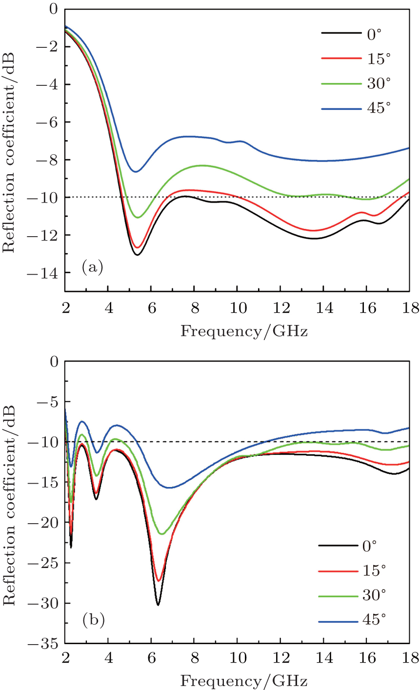 | Fig. 9. Curves of reflection coefficient versus frequency of (a) 2-layer absorber and (b) 7-layer absorber each backed by a PEC plate for different incident angles. |
Based on the stable performance in oblique incidence, the 7-layer absorber is predicted to be available also in the case of incline-like and camber-like backgrounds, which are the other two typical shapes of practical objects. Subsequently, the 7-layer absorber is coated on the surfaces of the PEC plate, pyramid and cylinder, respectively, and simulated in GEMS to verify the RCS reduction effect. The illustrations and dimensions of these three PEC backgrounds are shown in Fig. 10.
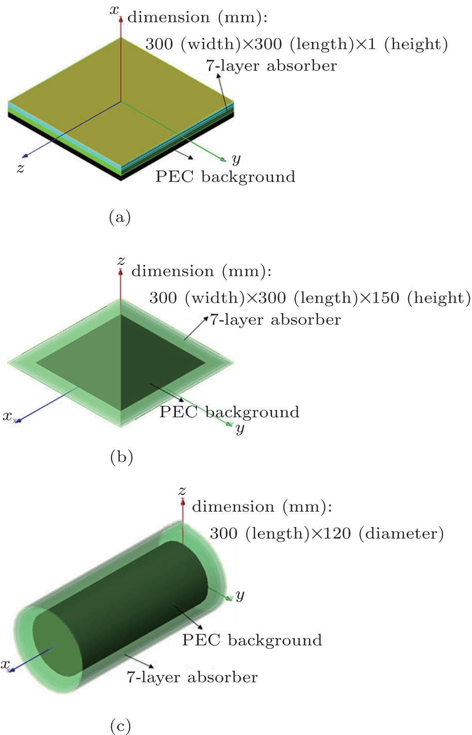 | Fig. 10. Illustrations of PEC (a) plate, (b) pyramid, and (c) cylinder covered with 7-layer absorber. |
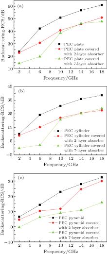
Figure 11 shows the backward scattering RCS spectra plotted against the frequency of these three PEC objects covered with the 2-layer and 7-layer absorber, respectively. For the plate and cylinder case, the backward scattering RCS is much more reduced by covering the 7-layer on the surface than by covering the 2-layer absorber in a frequency range of 2 GHz– 10 GHz, which is in accordance with the reflection coefficient characteristics of these two absorbers in the case of normal incidence. Particularly, the EMA performance of the 2-layer absorber is obviously deteriorated and the RCS reduction is less than 5 dB in most of the simulated frequency range for the pyramid case, in which the RCS reduction is determined by the oblique incident EMA performance of the absorber because of the 45° incline-like wall. Whereas, the RCS reduction of more than 10 dB is achieved by covering the 7-layer absorber on the surface not only in the plate and cylinder case but also in the pyramid case, which implies that the 7-layer absorber is available for objects of arbitrary shapes.
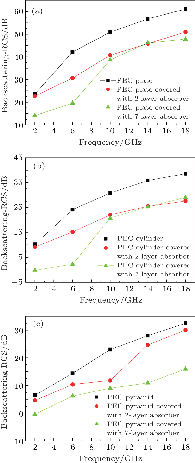 | Fig. 11. Variations of backward scattering RCS with frequency of PEC (a) plate, (b) pyramid, and (c) cylinder covered with 2-layer and 7-layer absorbers. |
In the present work, multilayer absorber with ultra wide effective absorption band is designed by the GA method. An ultra wide effective absorption band covering a frequency band of 4.6 GHz– 18 GHz is achieved in the 2-layer absorber with a total thickness of 3 mm. With the increase of layer number, the effective absorption bandwidth is broadened. The reflection coefficient of the 7-layer absorber backed with the PEC plate is smaller than – 10 dB in the whole frequency band of 2 GHz– 18 GHz, and the performance can be maintained in a wide incidence angle range of 0° – 30° . Moreover, the backward scattering RCS is reduced by at least 10 dB over the entire frequency band of 2 GHz– 18 GHz after coating the 7-layer absorber on the surface of the PEC plate, pyramid and cylinder.
| 1 |
|
| 2 |
|
| 3 |
|
| 4 |
|
| 5 |
|
| 6 |
|
| 7 |
|
| 8 |
|
| 9 |
|
| 10 |
|
| 11 |
|
| 12 |
|
| 13 |
|
| 14 |
|
| 15 |
|
| 16 |
|
| 17 |
|
| 18 |
|
| 19 |
|
| 20 |
|
| 21 |
|
| 22 |
|
| 23 |
|