Migration characterization of Ga and In adatoms on dielectric surface in selective MOVPE

Migration characterization of Ga and In adatoms on dielectric surface in selective MOVPE |
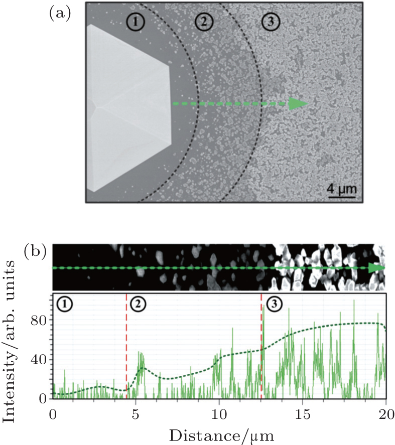
| (a) A high magnification SEM image of a μ-LED grown on 60-μm-period patterned template and its surrounding SiO2 mask. (b) EDS line analysis of the Ga Kα emission from region ① to region ③. |
 |