


Characteristics of charge and discharge of PMMA samples due to electron irradiation*
[Feng Guo-Baoa) , Wang Fanga)  , Hu Tian-Cun
b) , Cao Menga) ]
, Hu Tian-Cun|
|


†Corresponding author. E-mail: wangfang@mail.xjtu.edu.cn
*Project supported by the National Natural Science Foundation of China (Grant Nos. 11175140 and 11004157) and the Foundation of National Key Laboratory of Space Microwave Technology of China (Grant No. 9140C530101130C53013).
In this study, using a comprehensive numerical simulation of charge and discharge processes, we investigate the formation and evolution of negative charge and discharge characteristics of a grounded PMMA film irradiated by a nonfocused electron beam. Electron scattering and transport processes in the sample are simulated with the Monte Carlo and the finite-different time-domain (FDTD) methods, respectively. The properties of charge and discharge processes are presented by the evolution of internal currents, charge quantity, surface potential, and discharge time. Internal charge accumulation in the sample may reach saturation by primary electron (PE) irradiation providing the charge duration is enough. Internal free electrons will run off to the ground in the form of leakage current due to charge diffusion and drift during the discharge process after irradiation, while trapped electrons remain. The negative surface potential determined by the charging quantity decreases to its saturation in the charge process, and then increases in the discharge process. A larger thickness of the PMMA film will result in greater charge amount and surface potential in charge saturation and in final discharge state, while the electron mobility of the material has little effects on the final discharge state. Moreover, discharge time is less for smaller thickness or larger electron mobility. The presented results can be helpful for estimating and weakening the charging of insulating samples especially under the intermittent electron beam irradiation in related surface analysis or measurement.
Charging phenomenon and related effects of various insulating samples due to electron beam (e-beam) irradiation have been attracting a great deal of attention since they were first observed in the scanning electron microscope (SEM) to distort images in 1960s.[1, 2] Charging of specimen may not only degrade the accuracy of e-beam microanalysis, but also reduce dimension metrology and lithography.[3– 8] On the other hand, the accumulated internal charges will discharge by leaking to the grounded basement in the way of charge transport resulting from the internal built-in E-field and the charge density gradient.[9– 11] Hence, discharge presented by leakage current during the intermittence of electron irradiation will weaken charging effects. This occurrence of charge and discharge has significance in application fields of micromachining, space environment, and so on.[12– 15] Therefore, it is important to understand characteristics of combinational charge and discharge processes for reducing impacts of charging effects.
Charge as a result of e-beam irradiation and the subsequent discharge are related to the interaction between electrons and samples, and charge transport. Charging is caused by the imbalance between the inflow current, i.e., primary electron (PE) current, and the outflow currents, i.e., secondary electron (SE) and leakage electron currents. Due to the interruption of PEs, both PE and SE currents are absent, and only the leakage current continues during the discharge process.[16] Then, charge and discharge processes have intrinsic interrelation and dependence on parameters of electron irradiation and samples. Theoretical studies have simulated the charge process to obtain transient surface potential using radiation-induced conductivity (RIC) method with ignoring effects of SE emissions due to PE scattering and dynamic charging in the sample.[17– 20] Combining with Geant4 used in electron scattering, the RIC method is still appropriate on charge up effects in the space environment of high-energy (MeV) e-beam irradiation.[21] Some other works simulating PE scattering in insulator films with Monte Carlo (MC) method present the dynamic charging effect on SE emission during the charge process, [22, 23] showing the influence of SE emission on charge. Meanwhile, experimental researches usually examined currents and charge quantity of the PMMA film with certain sample parameters during charge and discharge processes under intermittent e-beam irradiation.[16, 17, 24] There still lacks studies concerning effects of related sample parameters on both charge and discharge characteristics, probably due to the difficulty in continuously changing the sample parameters in experiments. Therefore, a comprehensive simulation considering the scattering of PEs and the transport of internal charges is required to investigate charge and discharge processes to obtain characteristics of specimen charging states and effects from related sample parameters. As widely used in insulator, protection, and auxiliary materials, polymers are easy to be charged by e-beam because of their high-resistivity property.[18] Here, we take Polymethylmethacrylate (PMMA) as a representative insulation film sample to study its charging characteristics.
In this study, we numerically investigate charge and discharge characteristics of a PMMA film negatively charged due to non-focused e-beam irradiation. The electron scattering procedure in sample considering the emission of SEs is simulated with Monte Carlo method. The transport of charges accumulated in the sample is calculated by the finite-different time-domain (FDTD) method considering drift, diffusion, and trap of internal charges.[10, 25] The transient characteristics of internal currents, charge quantity, and surface potential during both charge and discharge processes are then obtained, as well as effects of sample parameters of thickness and electron mobility on charging intensity.
We first introduce the simulation model of the charge and discharge formation. Figure 1 shows the schematic of the charge induced by electron irradiation and discharge of PMMA sample. The PMMA film with the thickness H is placed on a grounded basement. The non-focused e-beam irradiates normally to the top surface of the sample. Considering that negative charging of an insulator sample can present more intense surface potential comparing with positive charging, the PMMA film is negatively charged with the surface potential VS < 0[26] by setting the PE energy EPE larger than the secondary cross energy in the curve of SE yeild, which is about 2.1 keV for PMMA material.[27]
 | Fig. 1. Schematic of electron irradiation on the grounded PMMA film with the electron mobility μ e and thickness H. JPE, JSE, JS, JL, and JD are the PE current, SE current, sample current, leakage current, and displacement current, respectively. |
Based on the continuity of electric current, the inflow current (PE current JPE) and outflow currents (SE current JSE and sample current JS), satisfy JPE= JSE + JS. JS obtained at the grounded bottom is constituted with the leakage current JL resulted by internal charge transport and the displacement current JD due to the induced electric field. The accumulated charges will be released in the form of leakage current JL towards the grounded basement under the force of internal built-in E-field.[28] When the quantity of internal charges in the sample reaches saturation, the displacement current JD disappears, so the electron currents balance as JPE = JSE + JL. To acquire complete charging characteristics during charge and discharge processes, the discharge process starts once the e-beam irradiation stops (JPE = 0). Accordingly, the charge process during electron irradiation consists of electron scattering and charge transport, while the discharge process only deals with charge transport after the irradiation. The electron scattering and transport processes are simulated in sequence because the former is much faster than the later.[19]
Electron scattering in PMMA, including the elastic and inelastic scattering, are simulated with the Monte Carlo method. In this simulation, the PE energy is set to be less than 10 keV. The Mott cross-section[29] is adopted to describe the elastic scattering as
 |
where σ is the Mott scattering cross-section, Ω and θ are solid angle and scattering angle, f (θ ) and g(θ ) denote the incident and the scattering wavelength division functions, respectively. Considering the complexity of calculating the Mott differential scattering cross section, we use the Mott scattering cross-section database[30] for different sample atoms, PE energy, and scattering angles. The total elastic scattering cross section can be obtained by
 |
The inelastic scattering cross section σ in is calculated with the fast secondary electron model[31] when the PE energy EPE is larger than 3 keV
 |
in which E is the incident electron energy, e denotes the absolute value of the electron charge, and Ω c is the minimum of normalized energy loss coefficient and set to be 0.001. The energy loss of inelastic scattering events is calculated with the modified Bethe energy loss formula by Joy and Luo[31]
 |
where the coefficient k is interpolated with the average atmospheric atom number Z̄ , Ā and J̄ are the average atomic weight and the average ionization energy, respectively, and ρ is the density of material.
When EPE is less than 3 keV, the inelastic scattering of electrons is more suitable to be calculated with the Penn model.[32] The corresponding inelastic differential cross section is represented by
 |
where λ in is the electron mean free path of inelastic scattering, Θ is the staircase function considering conservation of energy and momentum, Δ E is the electron transfer energy, Ep is plasma energy satisfying Ep = ℏ ω p, with ω p being plasma frequency, a0 is the Bohr radius, 
 |
where vF is the Fermi velocity. When the energy loss during each inelastic scattering event is larger than the band gap of material, an SE will be generated, leaving a hole in the sample. The SE will travel in the sample like a PE until it exhausts its energy or escapes from the sample surface.
Due to the elastic and inelastic scattering, some electrons deposit in the sample, while others can escape as the SEs.[33] To verify the electron scattering model for PMMA, the SE yield δ defined as the ratio of the number of SEs to the number of PEs, δ = NSE/NPE, is calculated and compared with experimental results. As shown in Fig. 2, the simulated δ depicted by a solid line for a PMMA sample with the flat surface is presented as a function of primary energy EPE, compared with the experiment result from Boudaya and Blaise.[27] Under the same neutrality surface potential, the agreement between simulation and experiment is obtained.
 | Fig. 2. Secondary electron yield δ as a function of primary energy EPE. Experiment results are plotted for comparison. |
The charge transport, including both the charge drift and diffusion caused by the build-in electric field and charge density gradient, are both taken into consideration in the charge and discharge processes. During the transport, some of the deposited charges may be trapped by trapping centers which widely exist in polymer materials.[34] The transport of holes are neglected for their low volume and velocity on charging.[19]
During the charge process, the variation of free electron density nF (t) in the sample with time t satisfies
 |
where terms with subscripts scat, drift, diff, and trap represent internal electrons distributions, drift, diffusion, and trap, respectively. The term (∂ nF/∂ t)scat in the charge process is calculated with the Monte Carlo method mentioned above according to different energies of irradiation electron. The landing energy of PEs is modified by the sample surface potential Eland = EPE− | VS| . Other terms in Eq. (7) satisfy
 |
 |
 |
where μ e is the electron mobility of the sample material, Ef is the build-in electric field intensity, De is the electron diffusion coefficient which is a function of μ e in the Nernst-Einstein relation as De = μ ekBT/e (kB is Boltzmann constant and temperature T = 300 K), nt is the density of trapped electrons in trapping center, τ F is the trap time constant of 1 s, and NT = 1.0× 1015 cm− 3 is the density of trapping center for PMMA, respectively.[18] In addition, the space potential V(z, t) inside the sample is calculated with the Poisson equation due to the sample net charge distribution as
 |
where the net charge distribution nNET (z, t) is obtained by considering hole distribution h(z, t), free electron, and trapped electron distributions as nNET (z, t) = h(z, t) − nF (z, t) − ntrap (z, t). The ɛ is the dielectric constant. The charge quantity per unit area Q(ti), accumulated in the sample at 0 < t < ti where ti is any moment in the charge or discharge process, and can be calculated by
 |
In the discharge process, since the inflow PEs stop, the term (∂ nF/∂ t)scat is set to be zero. Hence, according to Eq. (7), the variation of free electron density nF (t) with time t during the discharge process satisfies
 |
The surface potential V(z, t) and the charge quantity Q(ti) during the discharge process can also be calculated with Eqs. (11) and (12), respectively. During the whole charge and discharge process, the leakage current JL(t) satisfy the continuity equations JL(t) = − eμ enF (H, t)∇ V(H, t) + eDe ∇ nF (H, t), and the displacement current JD(t) can be calculated with JD(t) = ɛ ∂ (∇ V(H, t))/∂ t.
The whole simulation procedure including both charge and discharge processes is shown in Fig. 3. With the interruption of PE irradiation, the discharging process begins from the former charging states. The discharge process finishes with the disappearance of leakage current. Combining the scattering and the transport models, we simulate the evolution of internal currents JL(t), JD(t), surface potential VS(t), and total charge quantity Q(t) of the sample during both the charge and discharge processes. Simulations were carried out with default values of sample parameters as follows: the electron mobility of PMMA μ e = 1.0 × 10− 10 cm2· V− 1· s− 1, the sample thickness H = 10 μ m, the value of PE energy and current are set to be EPE = 10 keV and JPE = 50 nA· cm− 2, respectively.
 | Fig. 3. Solution procedure of charge and discharge processes. |
The transient properties of charge and discharge processes of PMMA are presented in Fig. 4. As shown in Fig. 4(a), due to the accumulation of the net inflow charges and the transport of internal charges, the leakage current JL emerges at 22 s. JL gradually reaches its maximum and then keeps dynamic balance at 40.5 s. Based on the continuity of electric current, the displacement current JD appears immediately at the beginning of irradiation. With the emergence and increase of leakage current JL, JD gradually reduces to zero when the internal charges accumulated become saturation within the charge duration I as illustrated in Fig. 4(a). In the discharge duration II, when PE irradiation stops, the leakage current JL gradually decreases to zero with the elapse of internal free charges. The displacement current JD drops to its negative maximum immediately at the very beginning of discharge duration and then gradually approaches zero, for the continuity of electric current as JL + JD = 0. The discharge time TC is defined as the duration from the beginning of discharge t0 to the moment that leakage current JL reaches 1% of its maximum t1 in the discharge process, TC = t1 − t0. Here, TC is ∼ 73.1 s according to this calculation.
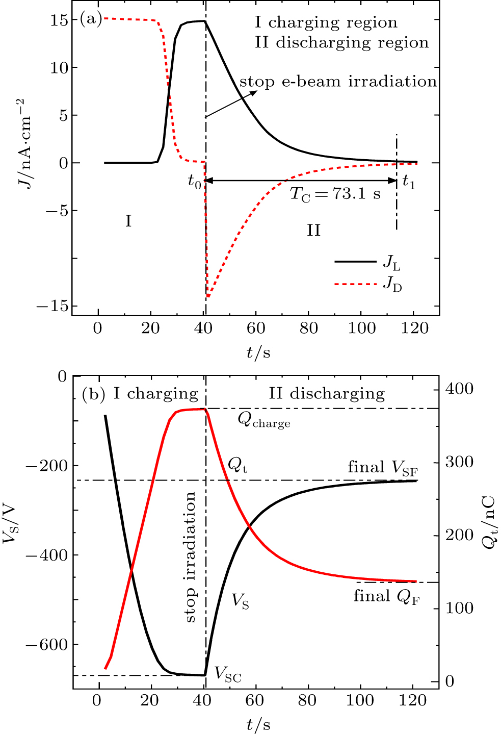 | Fig. 4. Transient characteristics of charge and discharge processes of the PMMA sample. (a) Variations of leakage current JL and displacement current JD with time t. TC is the discharge time. (b) Variations of internal charge quantity Qt and surface potential VS with time t. |
Due to variations of inflow and outflow currents, the charge quantity and surface potential of the sample will also change. According to Eq. (12), the charge quantity Qt can be integrated by displacement current JD. As shown in Fig. 4(b), the quantity of Qt increases with time t of irradiation until reaches its charging saturation Qcharge at the moment when JL reaches saturation in the charge process. In the discharge process, Qt decreases gradually to the final value QF. Since the de-trap process of trapped charges is negligible for its low volume and speed, the final internal charges QF in the discharge process is mainly composed of trap electrons. Accordingly, the discharge quantity in the form of leakage current JL can be calculated as Qdisc = Qcharge − QF. The ratio of discharge quantity rdis defined as rdis = Qdisc/Qcharge, is 0.63 according to the results in Fig. 4(b). Moreover, in the charge process, with the increase of internal charges Qt, the value of surface potential VS decreases and keeps a minimum VSC when Qt reaches saturation. When the electron irradiation stops, VS increases to its final value VSF which is determined by QF.
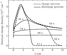
Figure 5 shows the distribution of sample internal charges in the z direction at different moments during the charge and discharge processes. Due to the drift, diffusion and trap, internal charges transport towards the sample bottom. The position of the maximum charge density related with electron scattering changes slightly in the charge process, as represented by dashed lines, in 11 s, 22 s, and 34 s. However, the maximum charges density decreases significantly and moves towards the sample bottom in the discharge process. With leakage of free charges in the discharge process, from the moment of 45 s to 88 s, the internal charge density decreases and finally approach an uniform distribution with the value of trapping center NT = 1.0× 1015 cm− 3.
 | Fig. 5. Internal charge distributions in the z direction at different times. |
We also simulate the charge and discharge processes for the PMMA sample of different thicknesses. The sample thickness H is 4– 20 μ m, widely used as a cover film. Figure 6(a) presents the negative charge quantity Q and surface potential VS, as functions of H. The charge quantity in saturation Qcharge and discharge quantity Qdisc increases with the increase of H. Qcharge is composed of trapped electrons and free electrons in the sample. Qdisc is almost from free electrons. As reported in our previous work, [25] the quantity of trapped electrons increase almost linearly with the increase of H, while the increase of free electrons with H is more slowly. Therefore, the increase of the sample thickness H results in more increase in Qcharge than in Qdisc as shown in Fig. 6(a). The discharge quantity ratio rdis then decreases with sample thickness H, as shown in Fig. 6(b).
 | Fig. 6. (a) Surface potential VS and charge quantity Q. (b) Discharge ratio rdis and (c) discharge time constant TC, as functions of the sample thickness H during charge and discharge processes. |
Moreover, as illustrated in Fig. 6(a), the surface potential in saturation VSC and surface potential in final state of discharge VSF decrease with the increase in H. The surface potential of the sample is stronger for thicker samples. Meanwhile, the difference between the surface potential in charging saturation VSC and in final state of discharge VSF, which is determined by discharge quantity Qdisc, increases with the increase in H.
As shown in Fig. 6(c), in thicker sample, free electrons need longer TC to leak to the grounded basement due to longer paths during the discharge process. The simulation results also show that the time constant TC increase with the increase of sample thickness H logarithmically as TC ∼ log (H).
The charge and discharge properties are also affected by electron mobility μ e of the sample. For PMMA, μ e can vary from 10− 9 to 10− 11 cm2· V− 1· s− 1.[18, 19] Figure 7(a) shows that the charge quantity in saturation Qcharge and the discharge quantity Qdisc decrease with the increase of μ e almost in the same amount. Larger electron mobility μ e makes free electrons leakage faster in the sample, which results in a less free charge quantity in charging saturation. Hence, both Qcharge and Qdisc decrease with μ e, and the surface potential in saturation VSC determined by Qcharge increase with μ e. Since the difference between Qcharge and Qdisc is mainly composed of trapped electrons, which is independent of μ e, the difference almost remains constant. Furthermore, the surface potential in the final state of discharge VSF determined by trapped electrons keeps invariable with μ e.
 | Fig. 7. (a) Surface potential VS and total charge quantity Q; (b) discharge ratio rdis and discharge time constant TC, as functions of the sample electron mobility μ e during charge and discharge processes. |
According to the variations of Qcharge and Qdisc shown in Fig. 7(a), the discharge quantity ratio rdis decreases with the increase of μ e, as shown in Fig. 7(b). Since larger electron mobility promotes the transport of free electrons, less time is needed for discharge process to reach its final states. Then, TC decreases with the increase of μ e, as illustrated in Fig. 7(b).
It should be noted that the discharge process in this simulation begins immediately after the charging reaches saturation. If the irradiation duration is extended, the charging saturation of sample will remain, and the discharging process after irradiation will be the same. If the interval of irradiation is shorter than the discharge time, the charge quantity and the surface potential of the sample will be stronger. In some cases, in order to weaken the charging effect, e-beam irradiation with an optimum interval estimated by this method is helpful. Moreover, some other parameters, such as trapping center density, temperature and permittivity, will also affect polymer charging.[35– 37] Further efforts could adopt this simulation method by taking more factors into account.
In summary, we have simulated and analyzed the charge and discharge characteristics of PMMA due to electron irradiation by a numerical simulation. The simulation shows that the charge accumulation by electron irradiation in the sample may reach charge saturation, and then decrease to their final states of discharge in which internal free charges dissipated and trapped electrons almost persist after stopping the electron irradiation. Although both charge and discharge quantities increase with sample thickness, but the discharge quantity ratio is less in a larger thickness sample. A PMMA sample with larger thickness or smaller electron mobility will have a stronger negative surface potential in the charge saturation. The surface potential derived from trapped electrons at the end of discharge is almost independent of electron mobility. Furthermore, the discharge time could decrease logarithmically with the decrease in sample thickness. Effects of sample thickness and electron mobility on the discharge time and the discharge quantity ratio can be considered for weakening charging under the intermittent irradiation. The results presented clarified the charge and discharge characteristics of the PMMA film due to internal charge transport and leakage, and the simulation method may help to predict the charging states for various samples.
We are sincerely indebted to our advisor Dr. H. B. Zhang (deceased), Professor of Xi’an Jiaotong University, for his long-term encouragement and advice.
| 1 |
|
| 2 |
|
| 3 |
|
| 4 |
|
| 5 |
|
| 6 |
|
| 7 |
|
| 8 |
|
| 9 |
|
| 10 |
|
| 11 |
|
| 12 |
|
| 13 |
|
| 14 |
|
| 15 |
|
| 16 |
|
| 17 |
|
| 18 |
|
| 19 |
|
| 20 |
|
| 21 |
|
| 22 |
|
| 23 |
|
| 24 |
|
| 25 |
|
| 26 |
|
| 27 |
|
| 28 |
|
| 29 |
|
| 30 |
|
| 31 |
|
| 32 |
|
| 33 |
|
| 34 |
|
| 35 |
|
| 36 |
|
| 37 |
|