


Photoactive area modification in bulk heterojunction organic solar cells using optimization of electrochemically synthesized ZnO nanorods
[Ahmadi Mehdi , Rashidi Dafeh Sajjad]
, Rashidi Dafeh Sajjad]
|
|


†Corresponding author. E-mail: m.ahmadi@vru.ac.ir
In this work, ZnO nanorod arrays grown by an electrochemical deposition method are investigated. The crucial parameters of length, diameter, and density of the nanorods are optimized over the synthesize process and nanorods growth time. Crystalline structure, morphologies, and optical properties of ZnO nanorod arrays are studied by different techniques such as x-ray diffraction, scanning electron microscope, atomic force microscope, and UV–visible transmission spectra. The ZnO nanorod arrays are employed in an inverted bulk heterojunction organic solar cell of Poly (3-hexylthiophene):[6-6] Phenyl-(6) butyric acid methyl ester to introduce more surface contact between the electron transporter layer and the active layer. Our results show that the deposition time is a very important factor to achieve the aligned and uniform ZnO nanorods with suitable surface density which is required for effective infiltration of active area into the ZnO nanorod spacing and make a maximum interfacial surface contact for electron collection, as overgrowing causes nanorods to be too dense and thick and results in high resistance and lower visible light transmittance. By optimizing the thickness of the active layer on top of ZnO nanorods, an improved efficiency of 3.17% with a high FF beyond 60% was achieved.
Organic solar cells (OSCs) based on the bulk heterojunction (BHJ) blend of a conjugated polymer and a fullerene derivative are becoming an alternative approach to clean and renewable energy resources, because of their advantages such as mechanical flexibility, low cost, light weight, and their easy solution-processed fabrication.[1– 8] Significant improvements in PSCs have been made in recent years via employing new materials, [9– 12] morphology control, [13] interface engineering, [8] and modifying fabrication processes.[5] Normal structure PSCs consist of a photoactive layer sandwiched between a low work-function metal cathode and a hole transporter layer of poly (3, 4-ethylenedioxythiophene):poly-(styrenesulfonate) (PEDOT:PSS) on top of an indium tin oxide (ITO).[13, 14] The acidic nature of PEDOT:PSS leads to demotion of the ITO electrode, [15] which dictates a large problem to device stability of PSCs.[16, 17] Another problem of the normal structure is the fast oxidation of the low work-function electrodes.[18]
The employing inverted structure is one of the strategies used for improving the device stability. Inverted devices, which employ electron transporter metal oxides for modifying ITO electrode and high work function metals as the top electrode, have been reported to exhibit much higher stability than normal ones.[19– 22] The inverted structure can demonstrate sustainable power conversion efficiency (PCE) even after long exposure to atmosphere conditions.[23]
A key component in the inverted PSCs is the electron-transporter layer material on the ITO electrode.[24] Inorganic transparent conductive oxides (TCOs), such as zinc oxide (ZnO) or titanium oxide (TiOx), which have been widely used as electron-transporter materials due to their solution process-ability and their electron selective properties. These properties originate from their conduction band edges that correspond well with the LUMO level of fullerene, the deep valence bands[25– 29] and capability to produce rigid, nanocrystalline structures. These structures present a direct and ordered path for generated electrons to the ITO electrode. A lot of crystalline structure TCOs such as templated porous structures, [30, 31] tetrapods, [32] or vertically aligned nanorods (NRs)[33– 42] were used as the electron acceptor. Among TCOs, ZnO is one of the most interesting materials because of its high electron mobility, [43] the availability of low temperature synthesis, and the potential to control the morphology.[41, 44]
Although impressive charge separation is obtained by a large superficial area between the electron donor and the acceptor, BHJ instruments usually suffer from a meandering and discontinuous charge transport path.[45] The introduction of vertically aligned inorganic nanostructures is one of the strategies for improving charge transport in the devices since they can act as nanochannels for low resistive electron transport paths with high carrier mobility. Since excitons can be separated not only at the interface between the electron donor and the acceptor but also at the interface between the electron donor and vertically aligned inorganic nanostructures.[46] ZnO has been of great interest in the preparation of such aligned one-dimensional (1D) structures due to its high electron mobility and easy availability at low temperature by controllable synthesis.[47] Previous works on the instruments consisting of aligned ZnO NRs mainly focused on the instrument performance influenced by the polymer infiltration, [48] ZnO morphology and synthesis chemistry, [38] different backing layers, [49] and post-treatments by different atmosphere.[50]
However, the fill factor (FF) of the polymer/ZnO NRs hybrid solar cells was mostly low due to the poor infiltration of polymer into the spacing of ZnO NRs.[48, 51– 54] Infiltration of a conjugated polymer into the ZnO NRs leads to a higher superficial area which in turn may increase the number of carriers extracted.[44] To investigate the role of ZnO NRs as an electron transporter in the nanostructured hybrid films, proper control experiments are crucial such as the dependence of the device performances on the length of ZnO NRs and on the thickness of the organic active layer.[37]
Until now, many physical and chemical techniques such as the vapour liquid solid method, [55] chemical vapour deposition, [56] hydrothermal growth, [57– 60] template method, [61] electrochemical deposition, [62] thermal evaporation, [63] and so on were used to fabricate ZnO NR arrays. Among these methods, electrochemical deposition (ECD) is a rapid, low temperature process compatible with different types of substrates, [64] cost-effective approach for the fabrication of ZnO NRs[65, 66] and produces highly crystalline nanowires or NRs with excellent electronic quality.[64]
In this study, we optimized the growth of ZnO NRs by modifying the length and density of the NRs at the surface via controlling the electrochemical process. We demonstrated a suitable ZnO NR morphology which is required for infiltrating an active layer into the NRs to make an optimized contact with them. We prepared parallel orientated ZnO NR arrays grown on the ZnO seed layer with the electrochemical method. The influence of the NR growth time on the morphology and optical properties of ZnO NR arrays has been investigated. In addition, different techniques such as x-ray Diffraction (XRD), scanning electron microscope (SEM), atomic force microscope (AFM), and UV– visible transmission spectroscopy were employed to characterize the ZnO NR arrays. The optimized ZnO NR arrays were successfully applied in a polymer solar cell based on the poly (3-hexylthiophene) (P3HT) and [6, 6]-phenyl C61-butyric acid methylester (PCBM) blend. In addition, we optimized the thickness of the active layer on top of ZnO NRs to improve the efficiency of the organic solar cells.
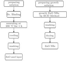
In this study, ZnO NRs were grown using a two-step process: (i) preparation of the seed layer via doctor blading and (ii) growth of the NR arrays by electrochemical deposition method.[67] First, the 0.1 mol/L seed layer solution was prepared by dissolving zinc acetate dehydrate in 2-methoxyethanol and stirring it for 2 h at 60 ° C and then 20-nm ZnO seed layer was coated via doctor blading on pre-structured ITO coated glass substrates followed by 1 h thermal treatment at 200 ° C to remove the residual organic solvents. The electrochemical deposition (ECD) of ZnO NRs was performed in a self-made two-electrode glass cell. The ECD cell was put into a water bath at 90 ° C during whole electrochemical deposition.
A pure silver sheet with an area of 2 × 2 cm2 was used as the anode electrode, ITO substrates (2 × 2 cm2) with the ZnO seed layer were used as the cathode, and electrolyte solution was 0.025 M zinc acetate dehydrate and hexamethylenetetramine aqueous solution without any supporting electrolyte. The deposition was performed at a constant current density of 0.2 mA/cm2. The growth time was 20, 40, 60, and 80 min. Finally, the as-prepared ZnO NR arrays were washed with deionized water and annealed at 200 ° C for 120 min. The procedure of this synthesis is summarized in Fig. 1.
 | Fig. 1. Schematic illustration for growth of ZnO NRs on the ZnO seed layer. |
In order to fabricate the organic solar cells, an active layer of P3HT:PCBM (1:0.9 wt%) prepared from chlorobenzene and with different thicknesses was doctor bladed on top of the ZnO seed layer/ZnO NR arrays. P3HT and PCBM were purchased from Merck and solenne BV, respectively. Afterward, around 20-nm-thick layer of poly (3, 4-ethylenedioxythiophene) polycationdoped with poly (styrenesulfonate) (PEDOT:PSS) diluted in isopropyl was bladed on top of the activelayer. The PEDOT:PSS solution was purchased from Clevios. The whole stack was annealed in inert atmosphere at 140 ° C for 5 min. At the end, a 100-nm-thick Ag layer was thermally evaporated on the PEDOT:PSS surface through a shadow mask to define an active area of 10.4 mm2.
Figure 2 shows the XRD patterns of ZnO seed-coated substrates suspended in solution with different growth time of 20, 40, 60, and 80 min. As shown in Fig. 2, there is no characteristic peak related to impurities of precursors such as zinc acetate. However, a very strong (002) diffraction peak and a very weak (101) peak are observed in the XRD pattern of ZnO seed layer suspended in solution with 40 min (Fig. 2(b)), indicating a high co-axis orientation of the ZnO NR arrays. In addition, the intensity of the (002) diffraction peak is the strongest, compared to other sample suspending durations. This result, in accordance with its SEM image of Fig. 3(d), implies its perfect co-axis orientation. For the ZnO NR arrays on the ZnO seed layer suspended for 60 min and 80 min, the (002) diffraction peak weakens while the (100) and (101) peaks slightly increase in strength, indicating its tendency toward random orientations. These conclusions closely match the SEM images of ZnO NR arrays observed in Fig. 3.
 | Fig. 2. XRD spectra of ZnO NRs grown on seed layer at 90 ° C for 20 min (curve a), 40 min (curve b), 60 min (curve c), and 80 min (curve d). |
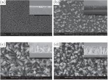
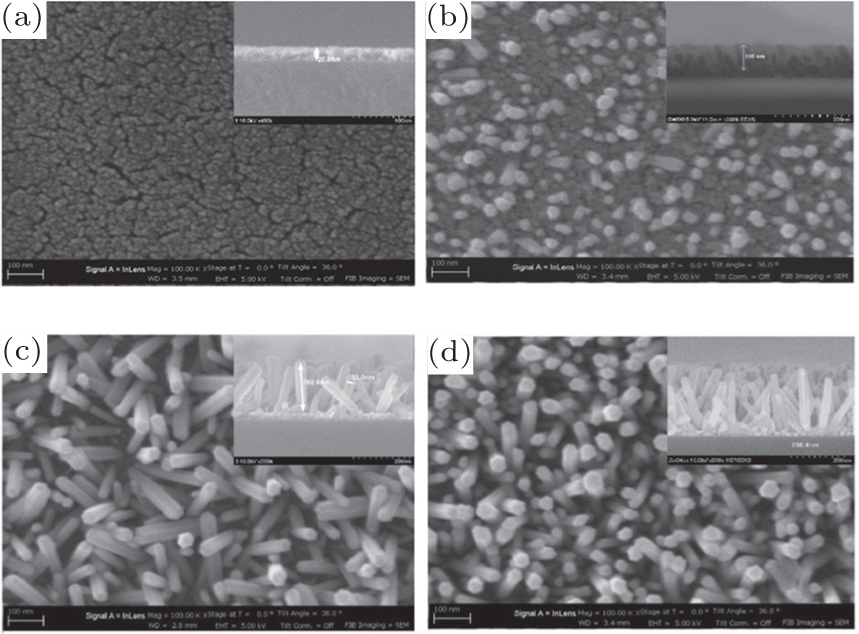 | Fig. 3. SEM micrographs of the ZnO NR arrays with (a) 20, (b) 40, (c) 60, and (d) 80 min suspending duration; the insets show the SEM cross-sectional view of ZnO NR arrays. |
Figures 3 and 4 show the SEM and AFM images of the ZnO NR arrays with different growth time. In Fig. 3(a), we can see that the growth of the NRs starts after 20 min but the length of them is very short. Figure 4(a) confirms this is due to the fact that the distance between the highest and the lowest points in the surface is about 30 nm.
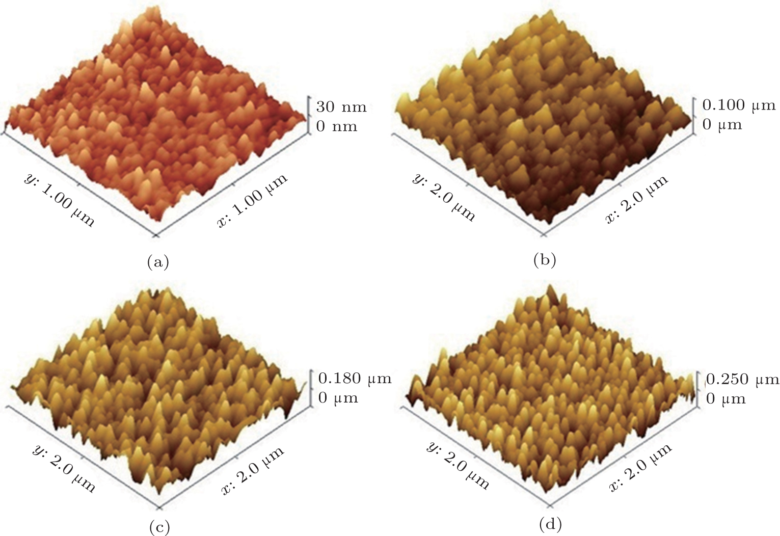 | Fig. 4. AFM images of the ZnO NRs with (a) 20, (b) 40, (c) 60, and (d) 80 min suspending duration. |
In Fig. 3(b), one can observe that after 40 min, ZnO NRs are grown clearly on the seed layer surface with a diameter of 20 nm. The cross section view in the inset shows the NR length of about 102.4 nm and figure 4(b) confirms it where the height of the highest point is around 100 nm. Figure 3(c) shows that after 60 min, ZnO NRs cover the surface with a much higher density. One can see from the inset of Fig. 3(c) that the length of the NRs reaches 180 nm after 60 min. The length of the NRs after 60 min observed by SEM image is in good agreement with the AFM image shown in the Fig. 4(c). According to the SEM image shown in Fig. 3(d), after 80 min, a very high dense ZnO NR array with the typical diameter of 30– 35 nm covers the surface completely and the inset picture shows that the NRs length is about 240 nm. Figure 4(d) indicates just a height of 240 nm between the highest and lowest points of the surface after 80 min.
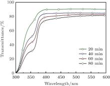
Optical properties of ZnO seed layer grown with various growth times of 20, 40, 60, and 80 min were studied by UV– vis spectroscopy measurement shown in Fig. 5. One can see that ZnO NR arrays are of high optical transmittance greater than 85%, for samples of 20 and 40 min growth time in the visible spectrum. The visible light transmittance decreases with the increase of the deposition time, since ZnO NR array films become denser with the increase of the diameter and the number of ZnO NRs.
 | Fig. 5. UV– vis spectra of ZnO NRs grown on seed layer at 90 ° C with 20, 40, 60, and 80 min suspending duration. |
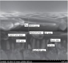
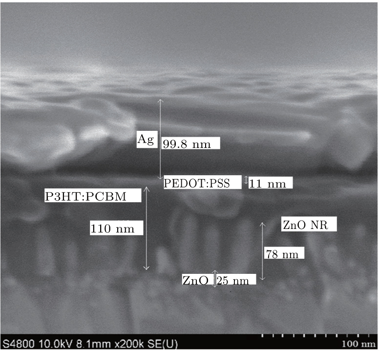
For the fabrication of the inverted organic solar cells, we select the ZnO NRs with 40-min growth time because of its suitable length and the density of the NRs to achieve a good infiltration of the active layer into the NRs. In addition, this choice leads to appropriate resistance and visible light transmittance. The J– V curves of the devices in the dark and under illumination are shown in Figs. 6(a) and 6(b), respectively. The device performance of key-parameters are summarized in Table 1. The device based only on the ZnO seed layer (ITO/ZnO seed layer/P3HT:PCBM/PEDOT:PSS/Ag) with an optimized thickness of the active layer yields power conversion efficiencies (PCE) of 2.91% with a short circuit current (Jsc), open circuit voltage (Voc), and fill factor (FF) of 9.07 mA/cm2, 0.54 V, and 59.55%, respectively. This performance agrees well with the values reported in the literature based on the P3HT:PCBM inverted device of the same structure.[36, 68] The cross-section SEM image presented in Fig. 7 shows that the employing of the ZnO NRs in the organic solar cell where ZnO NRs with a length of around 78 nm are embedded in the 110-nm-thick active layer of P3HT:PCBM. The optimized active layer thickness of 145 nm leads to the slight enhancement of PCE compared to the reference cell without NRs, based on the small improvement of Jsc, Voc, and FF, the optimized device achieved PCE of 3.17% with a Jsc of 9.44 mA/cm2, Voc of 0.55 V, and FF of 60.66%. It is worth mentioning that we are strongly limited to 100– 120 nm thick active layers, due to the material quality, to keep the FF as high as 60%. High efficient solar cells on the ZnO NRs with a FF over 60% for the active layer as thick as 145 nm could be an indication of the larger interfacial area for the charge separation and more efficient charge extraction. The larger interfacial area between the active area and the electron transporter layer minimized the distance charge carriers need to travel in the active area to reach the electrodes.[37, 50, 68]
 | Fig. 6. SEM cross section view of organic solar cells with ZnO NRs. |
| Table 1. Summarized performance key-parameters of the devices with various P3HT:PCBM thicknesses. |
The dark J– V curve (Fig. 6(a)) shows a higher injection current for the ZnO NR devices with 145-nm-thick active layer compared with the ZnO NRs with other active layer thicknesses and even the ZnO seed layer device. It could be an indication of the high conductivity of the ZnO NRs prepared in this condition. The light J– V curve (Fig. 6(b)) shows the Jsc improvement of the device with a 145-nm-thick active layer compared to the 110-nm-thick active layer. The FF is also slightly improved even compared to the reference of ZnO seed layer without NRs as well as the device on the ZnO NRs with 110-nm-thick active layer. Furthermore, the increase of the active layer to 200 nm is accompanied with a bit improved Jsc (9.58 mA/cm2) and significantly dropped FF (46.14%).
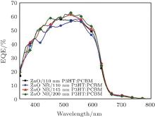
Figure 8 shows the external quantum efficiency (EQE) spectrum of the devices. The EQE reaches beyond 60% at the absorption peak of 530 nm for the samples of 145- and 200-nm-thick active layers on top of ZnO NRs, in complete agreement with J– V curves and summarized results in Table 1.
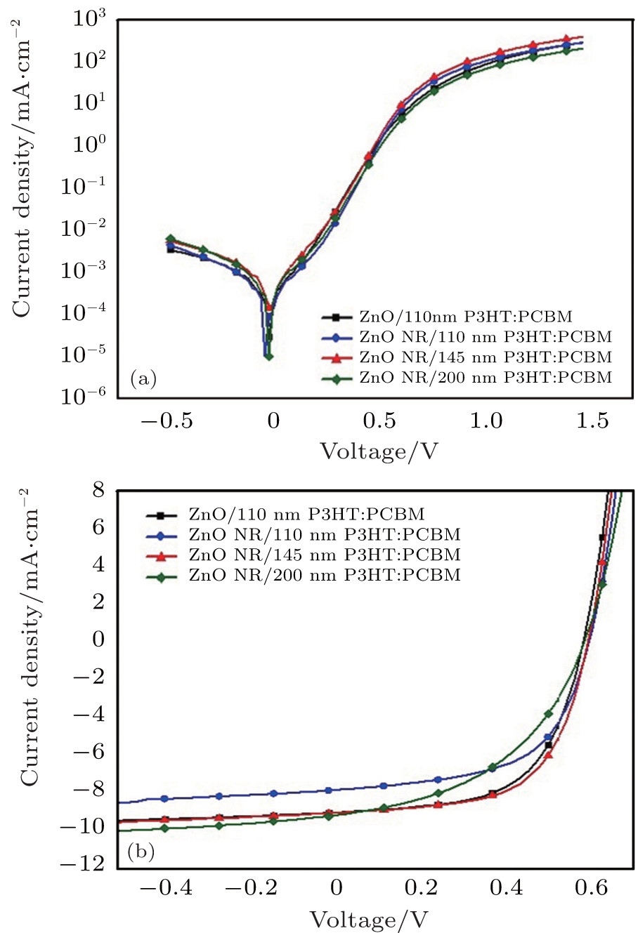 | Fig. 7. J– V curves of devices with various thicknesses of P3HT:PCBM (a) without illumination, (b) under simulated solar irradiation of AM1.5G. |
 | Fig. 8. Normalized EQE spectrum of the ITO/ZnO NRs/PCBM:P3HT/PEDOT:PSS/Ag device. |
Well-aligned ZnO NRs were synthesized successfully on the 20-nm-thick ZnO seed layer by the electrochemical method with different growth times, which led to different lengths and densities of ZnO NRs. As the growth time increases, ZnO NR arrays become denser and their diameter increases, which results in the increase in the resistivity of the films and a decrease in visible light transmittance. The characterization results of x-ray, SEM, and UV– vis transmittance spectroscopy verified the desired length, density, and optical transparency of the NRs grown on ZnO seed layer after 40 min. The achieved appropriate morphology of the ZnO NRs in 40 min led to the complete infiltration of the photoactive layer in ZnO NRs to make the maximum contact between the active layer and the button electrode in an inverted organic solar cell. Optimizing the thickness of the P3HT:PCBM active layer on top of ZnO NRs, an improved efficiency of 3.17% with a high FF beyond 60% was achieved.
| 1 |
|
| 2 |
|
| 3 |
|
| 4 |
|
| 5 |
|
| 6 |
|
| 7 |
|
| 8 |
|
| 9 |
|
| 10 |
|
| 11 |
|
| 12 |
|
| 13 |
|
| 14 |
|
| 15 |
|
| 16 |
|
| 17 |
|
| 18 |
|
| 19 |
|
| 20 |
|
| 21 |
|
| 22 |
|
| 23 |
|
| 24 |
|
| 25 |
|
| 26 |
|
| 27 |
|
| 28 |
|
| 29 |
|
| 30 |
|
| 31 |
|
| 32 |
|
| 33 |
|
| 34 |
|
| 35 |
|
| 36 |
|
| 37 |
|
| 38 |
|
| 39 |
|
| 40 |
|
| 41 |
|
| 42 |
|
| 43 |
|
| 44 |
|
| 45 |
|
| 46 |
|
| 47 |
|
| 48 |
|
| 49 |
|
| 50 |
|
| 51 |
|
| 52 |
|
| 53 |
|
| 54 |
|
| 55 |
|
| 56 |
|
| 57 |
|
| 58 |
|
| 59 |
|
| 60 |
|
| 61 |
|
| 62 |
|
| 63 |
|
| 64 |
|
| 65 |
|
| 66 |
|
| 67 |
|
| 68 |
|