†Corresponding author. E-mail: lxj0218@hit.edu.cn
*Project supported by the National Natural Science Foundation of China (Grant No. 51503053).
Owing to their unique structure and excellent electrical property, carbon nanotubes (CNTs) as an ideal candidate for making future electronic components have great application potentiality. In order to meet the requirements for space application in electronic components, it is necessary to study structural changes and damage mechanisms of multi-walled carbon nanotubes (MWCNTs), caused by the irradiations of 70 and 110 keV electrons. In the paper, the changes of structure and damage mechanisms in the irradiated MWCNTs, induced by the irradiations of 70 and 110 keV electrons, are investigated. The changes in surface morphology and structure of the irradiated MWCNT film are characterized using scanning electron microscopy (SEM), x-ray photoelectron spectroscopy (XPS), Raman spectroscopy, x-ray diffraction analysis (XRD), and electron paramagnetic resonance (EPR) spectroscopy. It is found that the MWCNTs show different behaviors in structural changes after 70 and 110 keV electron irradiation due to different damage mechanisms. SEM results reveal that the irradiation of 70 keV electrons does not change surface morphology of the MWCNT film, while the irradiation of 110 keV electrons with a high fluence of 5 × 1015 cm−2 leads to evident morphological changes, such as the formation of a rough surface, the entanglement of nanotubes and the shrinkage of nanotubes. Based on Raman spectroscopy, XPS, and XRD analyses, it is confirmed that the irradiation of 70 keV electrons increases the interlayer spacing of the MWCNTs and disorders their structure through electronic excitations and ionization effects, while the irradiation of 110 keV electrons obviously reduces the interlayer spacing of the MWCNTs and improves their graphitic order through knock-on atom displacements. The improvement of the irradiated MWCNTs by 110 keV electrons is attributed to the restructuring of defect sites induced by knock-on atom displacements. EPR spectroscopic analyses reveal that the MWCNTs exposed to both 70 keV electrons and 110 keV electrons suffer ionization damage to some extent.
Owing to their outstanding physical and chemical properties, carbon nanotubes (CNTs) are promising for many applications including weight structures for aerospace, advanced nanoelectronics, and various radiation detectors.[1– 3] It is a highlight that the CNTs-based nanoelectronic devices are considered to be more suitable for space applications.[4, 5] Nevertheless, the changes in microstructure and properties of the CNTs, induced by irradiation, are considerably complicated and still a challenging problem for their space applications. The electrons existing in the orbits designated as low earth orbit (LEO) have a widely varying energy spectrum ranging from tens of keV to GeV, [6] in which the keV-range electrons are the most significant components. Importantly, electrons less than 200 keV are not only large in amount but also sensitive to radiation effects on the CNTs. When an energetic electron hits the target, different mechanisms of damage creation can work. Depending on target material and incident particle characteristic, the main mechanism can be knock-on atom displacements, electronic excitations, ionization, etc. For CNTs, the considerable attention of previous studies[7– 9] was paid to the knock-on atom displacements caused by the keV-range electron. The incident electron energy is more than the threshold energy for knock-on displacing carbon atoms in the graphene structure. Early experiments[8] provided evidence that single-walled carbon nanotubes (SWCNTs) exposed to a focused 100 keV electron beam in a transmission electron microscope (TEM) are severely deformed locally, developing neck-like features along their bodies due to the removal of carbon atoms by knock-on displacements. Banhart et al.[9] also demonstrated that the electron focused beam with an energy of 300 keV and a current density of approximately 450 A/cm2 could lead to almost spontaneous shrinkage of all shells and even collapse of the multi-walled carbon nanotubes (MWCNTs) at 600 ° C, due to the loss of atoms and diffusion of the interstitials through the inner hollow in the axial direction. It is noteworthy that the above electron irradiation experiments were performed in situ in TEM where the irradiation-induced change in the atomic-level structure of an individual nanotube could be monitored. However, no analytical tool is versatile. TEM cannot be used to characterize the dangling bonds that can provide the evidence of electronic excitations and ionization on CNTs. So far, no reports have been given on the electronic excitations nor on electronic ionization, except knock-on atom displacements for the CNTs exposed to a focused electron beam in TEM.
Previously, low-energy electrons with less than the threshold energy in a vacuum were generally assumed not to cause damage to CNTs, and the electronic excitations and ionization effects seemed to be less important.[10, 11] However, in the last decade, Kanzaki et al.[12] and Suzuki et al.[13] have shown that SWCNTs are severely damaged by the irradiation of electrons having a much lower energy (20 keV) than the threshold energy of the knock-on damage (86 keV for an electron[14]). In such a case, electronic excitations are solely responsible for the defect formation. Previous literature[15, 16] indicated that low-energy electrons (below the threshold energy of the knock-on damage) do not change electric conductivities of MWCNTs. It seems that the electron excitations and ionization do not occur in MWCNTs. We believe that it might be too early to make such a conclusion now. In order to examine the relationship between properties and damage mechanism, more work needs to be done, especially in electronic excitation and ionization on the MWCNTs, induced by low-energy electrons (less than 200 keV), which have seldom been investigated until now.
The aim of this paper is to investigate the keV-range electron irradiation-induced damage mechanisms in the MWCNTs based on scanning electron microscopy (SEM), x-ray photoelectron spectroscopy (XPS), Raman spectroscopy, x-ray diffraction (XRD) spectroscopy, and electron paramagnetic resonance (EPR) spectroscopy. The obtained results would be helpful to promote the space application of the MWCNT film, since a large number of the keV-range electrons exist in space.
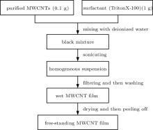
The MWCNT film used in this paper was provided by the National Center for Nanoscience and Technology of China. MWCNTs with a purity of about 95% were purchased from CNano Technology Limited Company, USA. The flow diagram for preparing the MWCNT film is shown in Fig. 1. Prior to the preparation of the film, the surfaces of MWCNTs are functionalized according to the following procedure. The 0.1 g purified MWCNTs and 1 g surfactant (TritonX-100) were mixed with 100 ml of deionized water, and sonicated by using an ultrasonic bath for 2 h. Afterwards, the mixture was turned into a homogeneous and black suspension. The black suspension under a pressure of 400 kPa from the suction filtration equipment was filtered by using a polytetrafluoroethylene (PTFE) membrane filter with a pore size of 0.2 μ m to make a wet MWCNT film. In order to remove the residual surfactant, the wet MWCNT film was washed repeatedly by using 400 ml deionized water and 200 ml methanol, respectively. Then, the wet MWCNT film was dried in a vacuum for 24 h at 100 ° C. After drying, a free-standing thick MWCNT film was obtained from the PTFE filter by peeling it off very carefully. The thickness of the MWCNT film was measured to be about 65 μ m by using a Form Talysurf PGI 1240-type profilometer. The purity of the MWCNT film is about 90% examined by a non-isothermal thermo-gravimetric analysis (TGA) (Model Q600SDT). In addition, in order to demonstrate whether there is the component of PTFE in the MWCNT film, x-ray photoelectron spectroscopy (XPS) analyses were conducted on the top and bottom surfaces of the MWCNT film. It is shown that the components of the two surfaces are the same, and the fluorine element of PTFE is not detected on the two surfaces as shown in Fig. 2. This result shows that the component of PTFE does not remain in the MWCNT film during the preparation of MWCNT film.
The electron irradiation experiments were carried out in a ground-based irradiation simulator at Harbin Institute of Technology, China. In order to study the keV-range electron irradiation-induced damage mechanisms in the MWCNTs, samples were perpendicularly irradiated by 70 and 110 keV electrons with 3 × 1011 cm− 2· s− 1 flux for fluences of 1 × 10¹⁵ and 5 × 1015 cm− 2, respectively. The test chamber was kept in a vacuum of 10− 5 Pa at room temperature.
In order to investigate the surface morphology, the pristine and the irradiated MWCNT film samples were observed by a field emission scanning electron microscope (FE-SEM, Model Quanta 200FEG, FEI, America). The chemical states of the pristine and irradiated MWCNTs were determined by XPS (Kα type, made by Thermo Scientific, USA) using an Al Kα source. X-ray diffraction (XRD) was examined on Philips X’ Pert to measure the structure parameters of all samples by using Ni-filtered Cu-Kα radiation in scanning steps of 0.02° at a scanning speed of 3° per minute. The quality of the pristine and the irradiated MWCNT film was analyzed based on Raman spectroscopy, using a LabRAM XploRA laser Raman spectroscope (HORIBA Jobin Yvon Co. Ltd.) with a 532-nm laser for an incident power of 1 mW. To further examine the characteristics of lattice defects caused by radiation damage, electron paramagnetic resonance (EPR) spectra of the pristine, and the electron irradiated samples were measured by using a Bruker A200 spectrometer (Bruker Instrument, Germany) in air and at room temperature, operating at a microwave power of 3.86 mW, a modulation amplitude of 1 G, and the time constant of 40.96 s. All EPR data were normalized to the specimen weight of 1 mg.
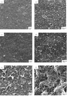
The SEM images of the pristine and the MWCNT film irradiated by 70 and 110 keV electrons are shown in Fig. 3. It can be seen from Figs. 3(a) and 3(b) that the surface of the pristine MWCNT film is rather smooth and compact with higher areal density of nanotubes. The outer diameters of the pristine MWCNTs are in a range from 110 to 135 nm as shown in Fig. 3(b). For the 70 keV electron irradiated MWCNT film, both at a low fluence of 1 × 1015 cm− 2 and at a high fluence of 5 × 1015 cm− 2, the surface morphologies have almost no change compared with those of the pristine sample, as shown in Figs. 3(c) and 3(d). For the MWCNT film irradiated by 110 keV electrons at a low fluence of 1 × 1015 cm− 2, it is observed that the surface morphology is the same as that of the pristine sample. However, as the incident electron fluence is further increased to 5 × 1015 cm− 2, the overall surface of the MWCNT film becomes quite rough (Fig. 3(e)), and the MWCNTs are more bent than the pristine MWCNTs. This may be due to the possible formations of pentagonal and heptagonal holes that are created by the irradiation and cause an expulsion of carbon from the graphene layer.[17] Moreover, the bended MWCNTs are entangled with each other (Fig. 3(f)). More interstices are formed and distributed between the entangled MWCNTs. The interstices can be formed by the displacements of the nanotubes from their initial positions. The above phenomena indicate that the surface morphology of the MWCNT film is greatly changed by the irradiation of 110 keV electrons with a high fluence of 5 × 1015 cm− 2.
It can be found from Fig. 3(f) that the outer diameters of MWCNTs irradiated by the 110 keV electrons with a high fluence of 5 × 1015 cm− 2 are much smaller than those of the pristine ones, indicating that remarkable dimensional changes occur in the MWCNTs. It seems that all nanotubes remain intact (no breakage or disintegration), although severe distortion takes place in the surface layer. The distortion could be related to shrinkage of the MWCNTs, caused by the 110 keV electrons. The shrinkage phenomenon of CNTs has been observed in situ in TEM by several groups.[7, 9, 18] Chopra et al.[7] have reported that after the prolonged electron irradiation with an 800 keV electron focused beam at room temperature, multi-walled tubes could be collapsed due to radial shrinking, leading to vanishing of the central hollow. Since the energy of 110 keV electrons used in this study is above the threshold energy of the approximate 100 keV for knock-on damage displacing carbon atoms in the graphene structure, [10] the major effect of the electron irradiation on the MWCNTs is the knock-on atom displacements caused by direct collisions between the incident electrons and carbon atoms. Therefore, it is believed that the removal of carbon atoms from a single-shell tube and the diffusion of the interstitials through the inner hollow lead to surface reconstruction and diameter reduction of the MWCNTs irradiated by 110 keV electrons with a high fluence of 5 × 1015 cm− 2. In contrast, 70 keV electrons are far below the threshold energy of 100 keV, indicating that the knock-on atom displacements could not happen in the CNT lattice, then no dimensional changes are observed for the MWCNTs as shown in Fig. 3(d). Based on the above SEM results, it is indicated that 110 keV electrons can remarkably reduce diameters of the MWCNTs, which strongly depends on irradiation fluence, while 70 keV electrons cannot change the diameters of the MWCNTs.
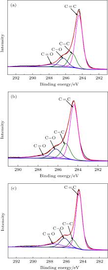
XPS is utilized to characterize the surface chemical compositions of the C (1s) core level of the pristine and irradiated MWCNT film as shown in Fig. 4. The spectra show a high peak at 284.4 eV, indicating the presence of C= C bond (sp2) on the surface and three smaller shoulders located at around 285.2 eV (C– C bond), 286.3 eV (C– O bond), and 287.5 eV (C= O bond). Table 1 summarizes the relative percentages of the different chemical states of C 1s for the pristine and irradiated MWCNT film by 70 keV and 110 keV electrons after XPS peak fitting and quantitative analysis. It can be known from Table 1 that the content of sp2 carbon decreases from 60.1% to 57.1% for the pristine and the irradiated MWCNT film by 70 keV electrons with a fluence of 5 × 1015 cm− 2, while that of sp3 carbon increases from 17.3% to 19.7%. The calculated ratios of sp2 hybridization to sp3 hybridization (C(sp2)/C(sp3)) for the pristine and the irradiated MWCNTs are 3.5 and 2.9, respectively. Moreover, the oxygen-contained composition content in the C (1s) increases from 22.6% to 23.2%. Therefore, sp2 structure in the C (1s) peak of the irradiated MWCNT film increases due to the decrease of sp3 bonds in the sample as compared to that of the pristine sample. This means that the quality of the irradiated MWCNTs increases by 70 keV electrons with the fluence of 5 × 1015 cm− 2. However, for the radiation of 110 keV electrons, the calculated ratios of C(sp2)/C(sp3) for the pristine and irradiated MWCNTs with the fluence of 5 × 1015 cm− 2 are 3.5 and 6.2, respectively. In addition, the oxygen-contained composition content in the C (1s) increases from 22.6% to 27.8%. The above results show that irradiation of 110 keV electrons can improve the structural quality of the MWCNTs. When energetic electrons with energy higher than the threshold energy for knock-on atom displacements hit the carbon atoms of MWCNTs, the most important mechanism is the displacement of carbon atoms due to kinetic energy transfer of energetic irradiation to carbon atoms. Moreover, sp2-bonded carbon systems are governed by knock-on atom displacements under the irradiation of electron or ion beams. According to the results, sp2 structure of the irradiated MWCNTs by 110-keV electrons can be increased due to the restructuring of defect sites induced by knock-on atom displacements.[10] It is worth noting that the oxygen compositions for the irradiated MWCNTs by 70 keV and 110 keV electrons increase, compared with the original sample. It might be believed that the amorphous carbon (sp3) in the irradiated MWCNTs could be easier to oxidize once the irradiated MWCNT film is exposed to air before the XPS testing, since the sp3 carbon has quite low bonding energy and relatively high reactivity induced by proton irradiation compared with sp2 structure.[19]
| Table 1. Relative percentages of the different chemical states of C 1s for the pristine and irradiated MWCNT film by 70 keV and 110 keV electrons with a fluence of 5 × 1015 cm− 2. |
Raman spectroscopy is a promising tool to characterize carbon materials and to evaluate disorders in their structures, because of its fast and nondestructive advantages.[20] Figure 5 shows the Raman spectra for the pristine and the irradiated MWCNT film by 70 and 110 keV electrons. Typical Raman spectra of the pristine and the irradiated MWCNTs films are similar. There are two sharp peaks at 1345 and 1584 cm− 1, assigned as D and G band, [21, 22] respectively. The D band is associated with vibration of the carbon atoms in disordered graphite, such as defects (vacancies, topological defects caused by forming pentagons and heptagons), dangling bonds in plane terminations, and other impurities. The G band corresponds to an E2g mode of graphite, which is relevant to the vibration of the sp2-bonded carbon atoms in a two-dimensional hexagonal lattice, indicating the presence of crystalline graphitic carbon in the MWCNT film. Normally, the ratio of D band intensity to G band intensity (ID/IG) can be calculated for characterizing the irradiated MWCNT films by 70 and 110 keV electrons as shown in Fig. 6. It is known that the smaller the ID/IG ratio, the higher degree of graphitization is expected in carbon material. It is noted that the changes of ID/IG values for the two irradiated samples with increasing the fluence are different. For the 70 keV-electrons-irradiated MWCNT films, ID/IG increases from 1.03 to 1.22 with increasing electron fluence from 0 to 5 × 1015 cm− 2, indicating that the number of defects in the MWCNTs is increased. However, for the irradiated MWCNT films by 110 keV electrons, ID/IG decreases from 1.03 to 0.92 with increasing the electron fluence, implying that the number of defects in the MWCNTs is reduced. From the above results, it is demonstrated that the irradiation of 70 keV electrons causes the damage to the structure of the MWCNTs, while the irradiation of 110 keV electrons can improve the structural quality of the MWCNTs, and the irradiation fluence plays a key role in increasing both the disorder and the order of the MWCNTs. These results are in good agreement with the results of XPS analysis. The opposite effects caused by the 70 and 110 keV electrons result from different damage mechanisms in the MWCNTs.
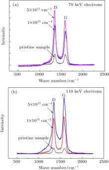 | Fig. 5. Raman spectra of the pristine and the irradiated MWCNT film by (a) 70 keV electrons and (b) 110 keV electrons. |
XRD is a sensitive method of characterizing the structural perfection of carbon material. The XRD patterns of the pristine and the irradiated MWCNTs by 70 and 110 keV electrons are shown in Fig. 7, indicating no distinct difference resulting from the variation of irradiation fluence. The main peak can be seen to occur at 2θ of approximately 25.6° , corresponding to the (002) reflection of the pseudo-graphite structure.[23] However, the enlarged patterns for (002) diffraction peaks of the two irradiated samples from 22° to 30° (the insets in Figs. 7(a) and 7(b)) indicate that the changes in (002) diffraction angles of the two irradiated samples are different as the irradiation fluence increases. For the irradiation of 70 keV electrons, the (002) diffraction peak shifts to lower angles, while the peak shifts to higher angles for the irradiation of 110 keV electrons with increasing the irradiation fluence. The d002 spacings of all the samples are calculated from Bragg equation (d = λ /2sinθ ), as listed in Table 2. It can be seen that the d002 interlayer spacing, the indication of the degree of graphitization, increases gradually from 0.343 nm for the pristine film to 0.346 nm for the film irradiated by 70 keV electrons at the high fluence of 5 × 1015 cm− 2, illuminating that the microstructure of the MWCNT film is broken partially by the irradiation of 70 keV electrons. On the contrary, the d002 interlayer spacing decreases gradually from 0.343 nm to 0.340 nm for the film irradiated by 110-keV electrons. In the latter case, the interlayer spacing (0.340 nm) turns closer to the ideal value of spacing of the graphite layer in a perfect graphite crystal (0.335 nm). This indicates that the degree of graphitization of the MWCNTs can be improved by the irradiation of 110-keV electrons. The result is in good accordance with that indicated in Ref. [24].
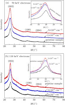 | Fig. 7. XRD patterns for the irradiated MWCNT film by (a) 70-keV electrons and (b) 110-keV electrons. The insets show the corresponding patterns from 22° to 30° (2θ ). |
| Table 2. XRD analysis results for the MWCNT film irradiated by 70 and 110 keV electrons. |
From the above XPS, Raman spectroscopy and XRD analyses, the irradiation of 70 keV electrons increases both the number of defects and the interlayer spacing in the MWCNTs, and disorders their structures. Contrarily, the irradiation of 110 keV electrons reduces the number of defects and interlayer spacing in the MWCNTs, and improves their graphitic order. These opposite effects are not surprising. Although the energy of 70 keV electrons is lower than the threshold energy of 100 keV for atomic displacements, they could cause ionization or bond breaking following electronic excitations in the MWCNTs. Since the C– C bond energy in a graphene sheet is only several eV, the energy of 70 keV electrons is high enough to break C– C bonds. It is reasonable that the low-energy electron irradiation could create defects with a certain probability if the defect structure is stable and the lifetime is long enough. It can be believed that even if the low-energy electrons cannot lead to atom displacements, they might also damage the MWCNT target because of local chemical reactions between nanotubes due to bond breaking and gaseous species such as water molecules, [25, 26] which results in an increase in the number of defects. As a result, the interlayer spacing increases since the defective graphenes typically have large interlayer spacing.[27] However, for the 110 keV electrons, the primary radiation effect on the MWCNT film is knock-on atom displacements, leading to the generation of vacancies and interstitials (or structural defects). Since the vacancies are almost immobile, they would induce bending and curvature of graphene layers as confirmed by SEM (see Fig. 3(f)). On the other hand, the interstitials are much more mobile and invoke the reconstruction of defect sites, [10] resulting in an improvement in the structure of the MWCNTs.
As is well known, EPR spectroscopy has an outstanding sensitivity and resolution in detecting radiation-induced modifications, such as vacancies, dangling bonds and conducting electrons. This technique has been extensively used to investigate radiation-induced modifications in carbon materials. Figure 8 shows the EPR spectra for the pristine and the irradiated film by 70 and 110 keV electrons. It can be observed that the EPR spectra for all the samples are similar in shape, and exhibit three components: (i) the wide peak assigned to magnetic impurities, which is related to the fact that the electronic spin is subjected to both the external magnetic field and the molecular field; [28] (ii) the narrow peak assigned to either amorphous graphite or paramagnetic impurities (localized defects, such as vacancies or dangling bonds); (iii) the broad peak assigned to the delocalized electrons over the conducting domains of carbon nanotubes. These results are in accordance with those in the previous investigations on the single-wall carbon nanotubes.[29] It is found from Fig. 8(a) that the height of the narrow peak of the irradiated MWCNT film by 70-keV electrons significantly increases with increasing irradiation fluence compared with that of the pristine MWCNT film, suggesting that the concentration of localized defects (such as vacancies or dangling bonds) increases in the MWCNTs. The localized defects should be mainly attributed to the formation of dangling bonds induced by the electron irradiation, since the generation of vacancies through the knock-on atom displacements could not occur in the irradiated MWCNTs by the 70 keV electrons below the threshold energy for knock-on damage. It means that the electronic excitations are solely responsible for the formation of the localized defects. The excited states caused by such low-energy electrons with 70 keV can cause local atomic bonding instabilities and rearrangement, leading to the bond breakage and the formation of dangling bonds. On the other hand, the amplitude of the right broad peak of the irradiated MWCNT film by 70 keV electrons increases with increasing irradiation fluence. This indicates that the delocalized electrons over carbon nanotubes also increase with increasing fluence, which could be attributed to the ionization mechanism induced by 70 keV electrons. Moreover, the broad peak broadens considerably with increasing fluence, indicating that the interaction of the uncoupled electronic spins with the localized magnetic moments tends to be enhanced abruptly. The above results could infer that the electric conductivity of the MWCNT film may be enhanced by the irradiation of 70 keV electrons. In Ref. [15], much lower energy (20 keV) is chosen as the energy for electrons, so that the electric conductivities of the MWCNTs with a diameter of 10 nm are unchanged before and after irradiation.
Figure 8(b) shows that the narrow peaks of the irradiation MWCNT film by 110 keV electrons change little compared with those of pristine MWCNT film, suggesting that the irradiation has almost no influence on the localized defects in the MWCNTs. It is of interest to note that the heights and widths of both the wide peak and the broad peak are significantly increased for a low fluence of 1 × 1015 cm− 2, implying that the irradiation of 110 keV electrons may enhance the molecular field of the MWCNTs[28] and also the delocalized electrons over carbon nanotubes. However, as the incident fluence is further increased to 5 × 1015 cm− 2, both the height and width of the broad peak of the MWCNTs decrease severely, and almost disappear, indicating that the number of delocalized electrons over carbon nanotubes decreases greatly. This could be attributed to the fact that the reaction of the carbon free radicals created by 110 keV electrons plays an important role in the case of smaller interlayer spacing. As demonstrated by XRD, the d002 interlayer spacing for the MWCNTs at the fluence of 5 × 1015 cm− 2 is smaller than that at the fluence of 1 × 1015 cm− 2. The above results also infer that the electric conductivity of the MWCNT film could be affected by the 110 keV electron irradiation, and the MWCNTs are sensitive to ionization damage to some extent, besides the damage due to knock-on atom displacements.
The above results reveal that the electron energy is an important parameter to influence the radiation damage mechanism for the MWCNTs. If the electrons have enough energy, like 110 keV, both the ionization and the atomic displacement effects can take place in MWCNTs. When the energy of the electrons is lower than the threshold energy for knock-on atom displacements, electronic excitations and ionization effects in the MWCNTs are dominant. Hence, it might be reasonable that the electric conductivity for the MWCNT film could be increased under the irradiation of low-energy electrons, unless the electron energies are too low to induce ionization in the film.
It is of significance to examine the radiation damage mechanisms induced by the keV-range electrons for MWCNTs. The effects of the irradiations of 70 and 110 keV electrons on the surface morphology and microstructure of the 65 μ m thick MWCNTs film are investigated by SEM, XPS, Raman spectroscopy, XRD and EPR spectroscopy. Experimental results show that both surface morphologies and microstructure of the MWCNT film can be changed under the irradiations of the electrons with 70 and 110 keV for different fluences, indicating that the energy and fluence of the keV-range electrons are two important parameters to dominate the damage mechanisms for the MWCNTs. Under the 110 keV electron irradiation, the diameters of MWCNTs decrease, the bent MWCNTs are entangled, the interlayer spacing of the MWCNTs decreases, the graphitic order of the MWCNTs is improved, and the number of delocalized electrons over carbon nanotubes changes. Under the 70 keV electron irradiation, the surface morphology of MWCNT film hardly changes, the interlayer spacing of the MWCNTs and the disordered structure are increased, and both the localized defects and the delocalized electrons are increased. It is believed that the 110 keV electron irradiation could mainly induce the atomic displacements accompanied by ionization effects in MWCNTs, while 70 keV electron irradiation could induce electronic excitations and ionization effects in the MWCNTs.
| 1 |
|
| 2 |
|
| 3 |
|
| 4 |
|
| 5 |
|
| 6 |
|
| 7 |
|
| 8 |
|
| 9 |
|
| 10 |
|
| 11 |
|
| 12 |
|
| 13 |
|
| 14 |
|
| 15 |
|
| 16 |
|
| 17 |
|
| 18 |
|
| 19 |
|
| 20 |
|
| 21 |
|
| 22 |
|
| 23 |
|
| 24 |
|
| 25 |
|
| 26 |
|
| 27 |
|
| 28 |
|
| 29 |
|


