


Composite behaviors of dual meminductor circuits*
[Zheng Ci-Yana) , Yu Dong-Shenga)  , Liang Yan
a) , Chen Meng-Keb) ]
, Liang Yan|
|


†Corresponding author. E-mail: dongsiee@163.com
*Project supported by the Fundamental Research Funds for the Central Universities, China (Grant No. 2013QNB28.)
This paper focuses on analyzing the composite dynamic behaviors of two meminductors in serial and parallel connections with different polarities. Based on the constitutive relations, two time-integral-of-flux (TIF) controlled meminductors are adopted to theoretically demonstrate the variation of memductance in terms of TIF, charge, flux, and current. By utilizing a floating memristor-less meminductor emulator, the theoretical analysis reported in this paper is confirmed via a PSPICE simulation study and hardware experiment. Good agreement among theoretical analysis, simulation, and hardware validation confirms that dual meminductor circuits in composite connections behave as a new meminductor with higher complexity.
In the year of 1971 and 1976, Chua, [1] Chua and Kang[2] predicted the existence of the fourth two-terminal fundamental circuit element out of existing ones (resistor, inductor, and conductor). This new element is called a memristor (MR), whose mathematical model is based on the charge– flux relationship. The research work of the MR did not draw enough attention until May 2008, when the HP lab managed to find a nanoscale solid-state device possessing the properties of an MR.[3] In 2009, the definitions of meminductive and memcapacitive systems were extensively brought forward and then the special cases of memcapacitors (MCs) and meminductors (MLs) were symmetrically described.[4] Pinched hysteretic loops, regarded as a typical fingerprint of MR, MC, and ML, are also depicted in detail in Ref. [5].
Unlike the MR, there are no practical nano devices capable of characterizing ML and MC, thus many emulators have been proposed to mimic ML and MC for further research. However, many of the existing ML models possess disadvantages more or less, such as, being hard to fabricate, or application complexity, or grounded restriction. For instance, an anolog ML emulator has been constructed on the basis of an MR emulator consisting of a light-dependent resistor (LDR), [6] and this ML emulator can be easily implemented in practical circuit but has grounded restriction. In Ref. [7] an ML emulator without employing any memristive system was designed, however, only SPICE simulation was given for validation. Meanwhile, many effective mutators were proposed to transform MR into an ML or a meminductive system: in Refs. [8] and [9], universal mutators to transform a grounded MR into a floating ML were reported, although no practical experiment was given; in Ref. [10], a mutator to transfer an MR into a meminductive system with floating terminals was proposed and its relevant practical implementation was presented. The MR-based circuit may render the newly-built ML much complex. Recently, in Ref. [11], there has been proposed a practical floating flux-controlled ML emulator without requiring any MR.
Many research efforts have focused on probing the dynamic behaviors of circuits containing one single mem-element, such as manifolds of non-isolated equilibria of mem-circuits, [12] the responses of ML under various current excitation signals like DC, sinusoidal, and periodic current signals, [13] the behavior of MC under step and sinusoidal voltage excitations[14] and so forth.
On the other hand, the dynamic behaviors of circuits containing more than one MR element have already been studied. It is shown in Refs. [15] and [16] that compared with the connection of a single MR, composite connections of two MRs, or an MR in parallel with an inductor or a capacitor can generate diversified dynamic behaviors. Based on Ref. [15], in Ref. [17] the dynamic behaviors of composite MRs were studied with taking the coupling effect between two MRs into consideration. However, the dynamic behaviors of multiple MLs connected together have not fully been studied yet. Unlike MR, ML is a dynamic element with the ability to store energy. Circuits containing one ML with resistors or MRs are characterized as the first-order dynamic circuits. However, composite behaviors of dynamic circuits containing dual or more MLs are rarely discovered and undeniably deserve more concerns.
In addition, to probe the dynamic behaviors of composite MLs can facilitate the development process of ML-based application circuits. Until now, research interests related to potential applications of MLs include designing adaptive filters with controllable inductance, [18] building a chaotic signal generator, [19] implementing digital low-power computation[20] and fast computation.[21]
In the present work, inspired by the work about composite MR circuits, dynamic behaviors of two MLs in serial and parallel connections with different polarities are discussed innovatively. The rest of this paper is organized as follows. In Section 2, a brief description of a single ML is introduced. In Section 3, MLs in serial connections with two different polarities are discussed. Furthermore, an additional inductor is serially added to this serial ML circuit in order to further testify its dynamic characteristic. Similarly, in Section 4, results of MLs in parallel connections with two different polarities are given, along with an extra inductor in serial connection. In Sections 5 and 6, a practical time-integral-of-flux controlled ML emulator is used to validate the theoretical analysis by using PSPICE simulation and hardware experiment, respectively. In Section 7, concluding remarks are presented.
As previously defined by Chua, the basic constitutive variables of MR are charge q and flux φ , which are the integral of current and voltage, respectively. The integration enables MR to have the ability to memorize the past circuit history.[1] There exist different ways to define the constitutive relations of ML, one is stated in Ref. [22], which continues to take charge q and flux φ as two variables, the other is stated in Ref. [4], showing that by defining ρ as the time integral of flux (TIF), meminductive systems can be divided into charge-controlled and ρ -controlled ones. The basic relations between voltage and flux, flux and ρ can be written as follows:
 |
By using LM and 
| Table 1. Definitive equations of two different kinds of MLs. |
From Table 1, we can see that MLs can be classified as charge-controlled and ρ -controlled MLs. In this paper, we only take the ρ -controlled ML into consideration.
As defined in Table 1, the current, inverse meminductance, flux, charge, and the ρ are related by
 |
 |
Obviously, from Eq. (2), LM can be detected by measuring the slope of the φ – i curve. According to Eqs. (2) and (3), a ρ -controlled ideal meminductive system with two MLs can be defined by
 |
 |
 |
In Refs. [6]– [11], several SPICE emulator circuits have been proposed to mimic the dynamic behaviors of ML. For the sake of analysis simplicity, the ρ -controlled ML in Ref. [11] is taken into account, of which the inverse meminductance is in proportion to TIF with coefficient α , namely
 |
where β is the initial value of 
 |
 |
In the following sections, two MLs described by Eqs. (8) and (9) are used for analyzing the composite behaviors of dual ML based circuits.
Figure 1 shows the symbol of a single ML. There are several ways to connect dual MLs in a circuit. Firstly, the scenario of two MLs connected in series with different polarities is discussed in this section.
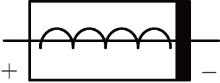
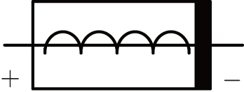 | Fig. 1. The symbol of a single ML. |
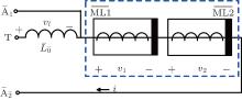
Figure 2 shows the schematic diagram of two MLs connected in series with identical polarities. When the input excitation voltage v12 is applied to this serial circuit between terminals A1 and A2, according to Kirchhoff’ s voltage law (KVL), the voltage and current relation of each ML can be expressed as
 |
 |
 | Fig. 2. MLs connected in series with identical polarities. |
By integrating both sides of Eq. (10), relations between the two fluxes can be presented by
 |
where φ 1 and φ 2 are the time integrals of v1 and v2, respectively. In addition, by integrating both sides of Eq. (12), the following relation can be obtained:
 |
By combining Eqs. (8), (9), and (11), the expression of current can be calculated by
 |
Based on Eq. (14) and assuming the initial value of ρ to be zero, we can obtain
 |
From Eq. (13), ρ 2 can be replaced by (ρ 12– ρ 1), thus we can obtain the following equation:
 |
Equation (16) is a second-order resolvable equation with unknown variable ρ 1. The analytical expressions of ρ 1 and ρ 2 can be rewritten by
 |
 |
If we take the special case of α 1 = α 2 = α for demonstration, equation (16) can be simplified into
 |
As a result, the expressions of ρ 1 and ρ 2 can be simplified into
 |
 |
Therefore, the inverse meminductance of individual ML can be obtained by substituting Eqs. (20) and (21) into Eqs. (8) and (9) respectively, leading to
 |
 |
For further simplification, we assume β 1 = β 2 = β , which leads to
 |
According to Eq. (24), we can obtain that
 |
For two serially connected inductors L1 and L2, their composite inverse inductance is supposed to be 1/(L1+ L2). Similarly, in an MLs’ s circuit, the composite inverse meminductance can be calculated from
 |
Thus, the composite inverse meminductance can be induced based on Eq. (25) as follows:
 |
Obviously, when connected in a series with identical polarities, two MLs can surely be operated as a new ML, which has linear ρ -controlled inverse meminductance.
In this subsection, two MLs connected in a series with opposite polarities are taken into account as shown in Fig. 3. When the input excitation voltage v12 is applied to this serial circuit between terminals A3 and A4, the voltages, fluxes and the values of ρ can be related by
 |
In this scenario, the expression of current leads to
 |
Similarly, by integrating both sides of Eq. (29) and substituting ρ 2 by (ρ 12– ρ 1), the following equation can be obtained:
 |
This equation can be analytically solved as
 |
 |
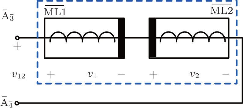 | Fig. 3. MLs connected in a series with opposite polarities. |
Likewise, by setting α 1 = α 2 = α and β 1 = β 2 = β , ρ 1 and ρ 2 can be simplified into
 |
 |
Hence, the inverse meminductance of an individual ML can be obtained by substituting Eqs. (33) and (34) into Eqs. (8) and (9) respectively, leading to
 |
 |
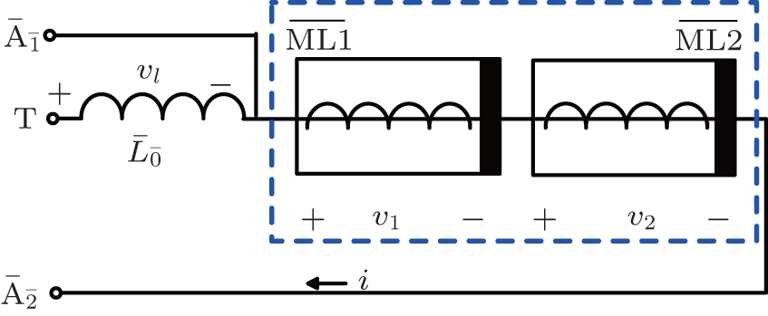
To further investigate the dynamic behavior of dual MLs connected in a series, an extra inductor L0 is adopted in serial connection with these two MLs as depicted in Fig. 2. The input voltage v12 is now applied between terminals T and A2. The voltages, fluxes, and values of ρ can be related correspondingly by
 |
The current flowing through each circuit element is
 |
By substituting Eq. (38) into Eq. (37), we have
 |
Then the value of the current can be represented as
 |
Thus the expression of flux can be written as
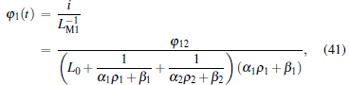 |
 |
 |
In view of Eq. (6), the expression of ρ can be calculated through the integration of the flux. However, equations (42) and (43) can be hardly resolved analytically. By taking into account the special case of α 1 = α 2 = α and β 1 = β 2 = β , and considering Eq. (24), the values of ρ for two MLs are the same
 |
 |
Consequently, the expression of ρ is
 |
The expression of the composite inverse meminductance can be obtained by substituting Eq. (46) into Eqs. (8) and (9), then calculated through Eq. (26) as
 |
In this section, MLs are configured in parallel connections in consideration of two different polarity cases.
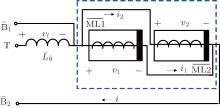
As is depicted in Fig. 4, ML1 and ML2 are connected in parallel with identical polarities. For parallel connections, when the input voltage v12 is applied between terminals B1 and B2, the voltages, fluxes, and values of ρ can be related correspondingly by
 |
 | Fig. 4. MLs connected in parallel with identical polarities. |
According to Kirchhoff’ s current law (KCL), the total current i is equal to the sum of i1 and i2, namely
 |
By substituting Eqs. (4) and (5) into Eq. (49), we have
 |
Then we integrate both sides of Eq. (50) by considering the special initial value condition of charge equal to zero, and obtain
 |
According to Eq. (3), the inverse composite meminductance can be obtained by taking derivatives of Eq. (51), and the calculated result is
 |
From Eq. (52), we can draw the conclusion that MLs in parallel connections can also be recognized as a new ρ -controlled ML with inverse meminductance equal to the sum of two individual inverse meminductances. Equation (52) is in good agreement with the expected theoretical results of two parallel connected MLs as 
When two MLs are connected in parallel with opposite polarities as shown in Fig. 5, and the input voltage v12 is applied to terminals B3 and B4, the relations among voltages, fluxes and values of ρ are the same as those presented in Eq. (48). Likewise, the relation between currents is identical to that in Eq. (49). Owing to the opposite polarities of MLs, the expression of total current can be obtained by substituting Eqs. (4) and (5) into Eq. (49), the results are
 |
By integrating both sides of Eq. (53) we have
 |
Using Eqs. (54) and (3), the total meminductance of MLs in parallel connection with opposite polarities can be calculated as
 |
 | Fig. 5. MLs connected in parallel with opposite polarities. |
For the further investigation of the dynamic of a parallel circuit, an additional inductor is considered in the connection. As shown in Fig. 4, the voltage v12 denotes the voltage imposed on terminals T and B2. The currents, voltages, and fluxes can be related correspondingly by
 |
The composite inverse meminductance of two MLs connected in parallel is shown in Eq. (52). Taking into account that i = φ /L and by considering Eq. (56), the relation of fluxes can be written as
 |
By integrating both sides of Eq. (57), the following equation holds:
 |
Thus, the expression of ρ can be solved as
 |
The expression of the composite inverse meminductance can be obtained by substituting Eq. (59) into Eq. (52), namely
 |
In order to validate the theoretical analysis, by referring to a previously proposed ML emulator, [11] the PSPICE model of a single ML, which is then used to establish the dual MLs circuit, is shown in Fig. 6, where A and B are two ports for this element to connect in a circuit. Owing to the difficulty in capturing the values of charge in the practical circuit implementation using PSPICE and hardware, here, flux and current are chosen as two variables instead of ρ and q, which are also in good agreement with the constitutive relation of ML.
 | Fig. 6. Pspice model of a single ML. |
In this emulator circuit, vci = vφ and vci is proportional to the time integral of current ici flowing out from terminal 5 of U1. Owing to the input– output characteristics of the circuit component AD844, the current flowing into terminal 2 is invariably conveyed to the output terminal 5. Besides, the voltages of terminals 2, 3, and 5 are the same. Thus, the voltage applied between terminals A and B is identical to the voltage across nodes C and D, namely, vAB = vRi = vci = vφ . The equation of vci is
 |
Obviously, vci is proportional to flux φ , thus the value of vci can be used to represent that of φ . The flux can then be calculated as φ = vciRiCi = vci × 10− 2.
Moreover, the output voltages of U5C and U6C can be expressed as
 |
 |
The value of inverse meminductance can be identified as
 |
where

Note that the value of 


As is well known, mem-elements can store historic information, so the initial values of inverse meminductace for two MLs are possibly different. In the simulation process, we set the initial inverse meminductance values of two MLs to be β 1 = 0.09 H− 1 and β 2 = 0.05625 H− 1. Meanwhile, the values of α 1 and α 2 are configured as α 1 = α 2 = 235.29412. As for the supply voltage v12, we adopt a sinusoidal input signal v12(t) = 5.75sin(73.8π t) to excite the dual ML circuit.
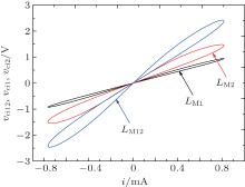
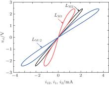
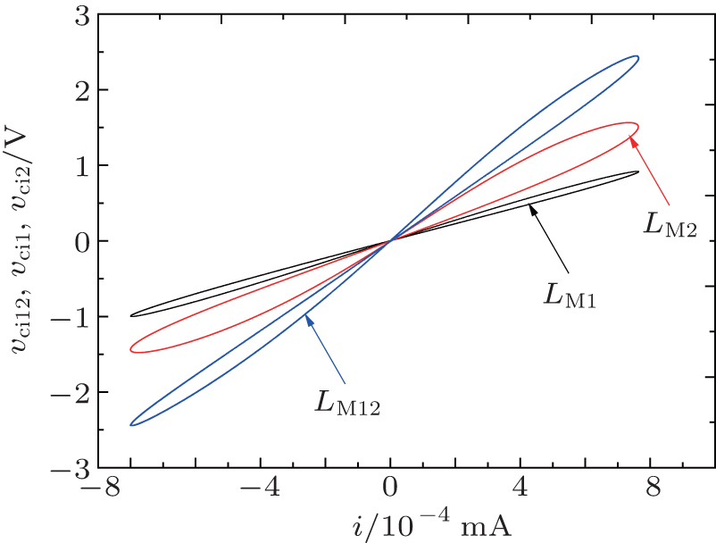
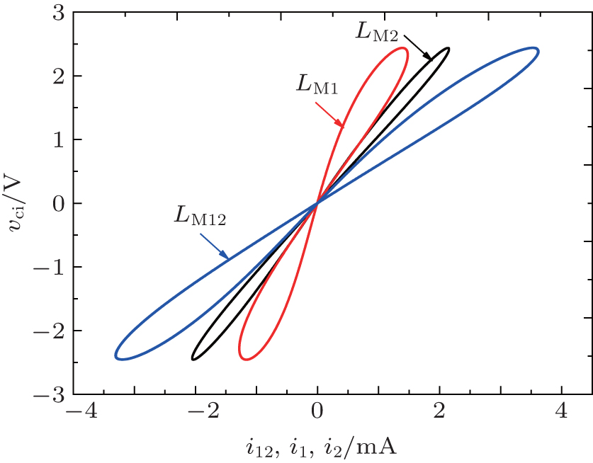
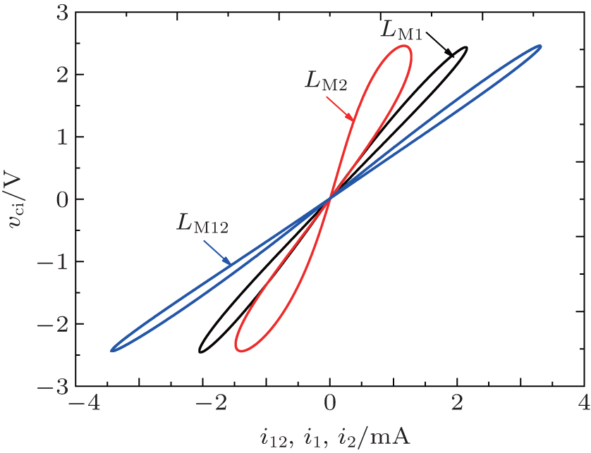
As is well known, the flux, inductance, and current flowing through an inductor are related by L = φ /i. Figure 7 shows the relationships between current (i) and the equivalent flux corresponding to two individual MLs and the serial ML circuit (ν ci1, ν ci2, ν ci12). The slope of the curve can be used to represent the instant value of the composite meminductance value. It can be clearly seen that the two serial MLs and their composite ML possess meminductive characteristics with typical nonlinear pinched hysteresis loops behaving as an inclined “ 8” , which differs from the behavior of a linear inductor. For the reason that the relation among LM12, LM1, and LM2 in serial connection can be described as LM12 = LM1+ LM2, here, the value of the composite LM12 is larger than those of LM1 and LM2. Thus the slope of the φ 12/i curve, which denotes the value of LM12, is steeper than those denoting the values of LM1 and LM2 for any given current.
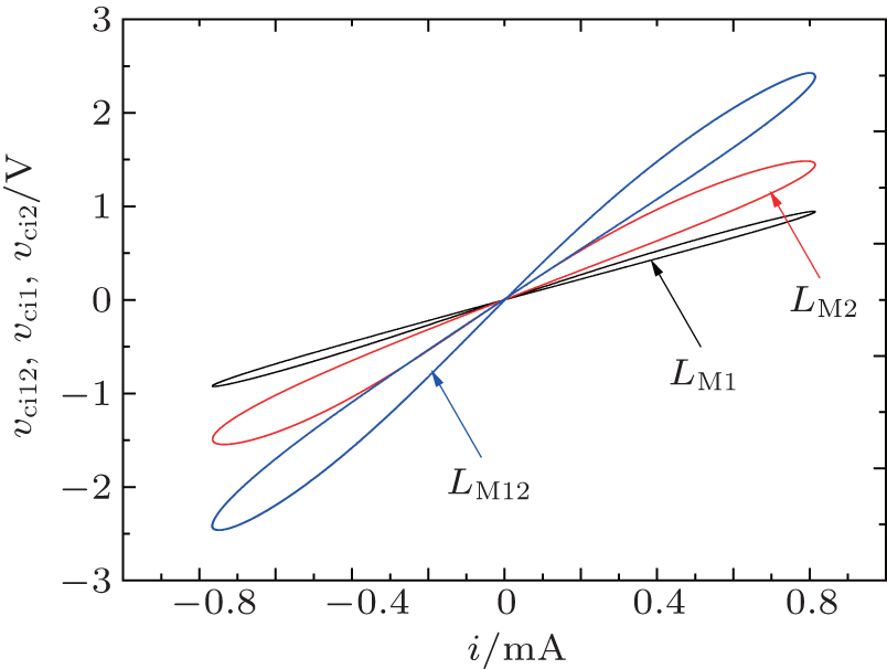 | Fig. 7. Simulation results of pinched hysteresis loops for MLs connected in series with identical polarities. |
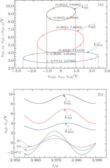
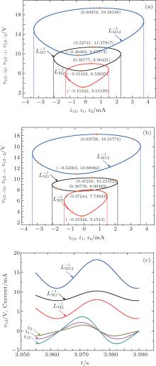
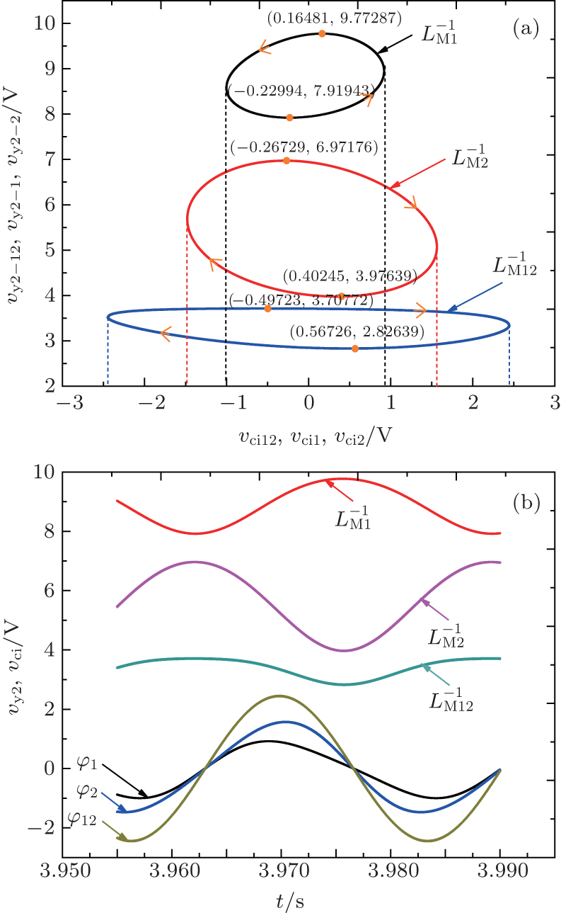
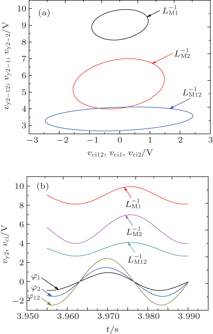
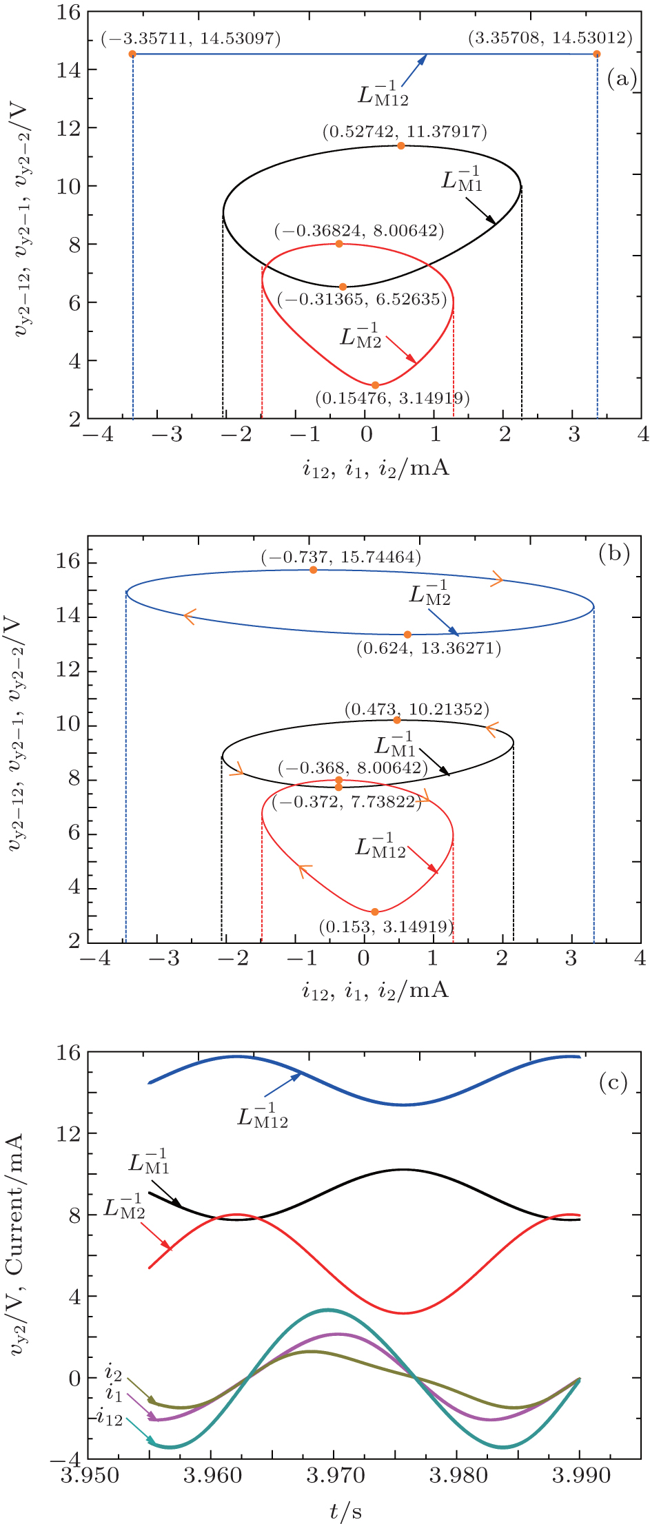
Figure 8 shows the relationships between the equivalent flux and inverse meminductance corresponding to two individual MLs and the serial ML circuit (vci1, vci2, vci12 and vy2− 1, vy2− 2, vy2− 12). It can be seen from Fig. 8(a) that there are two values of the equivalent inverse meminductance corresponding to each given flux. Evidently, the changing flux range of LM2 is wider than that of LM1. The reason is that according to Eq.(7), the inverse meminductance value is related to the initial value 


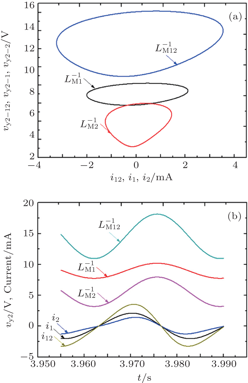
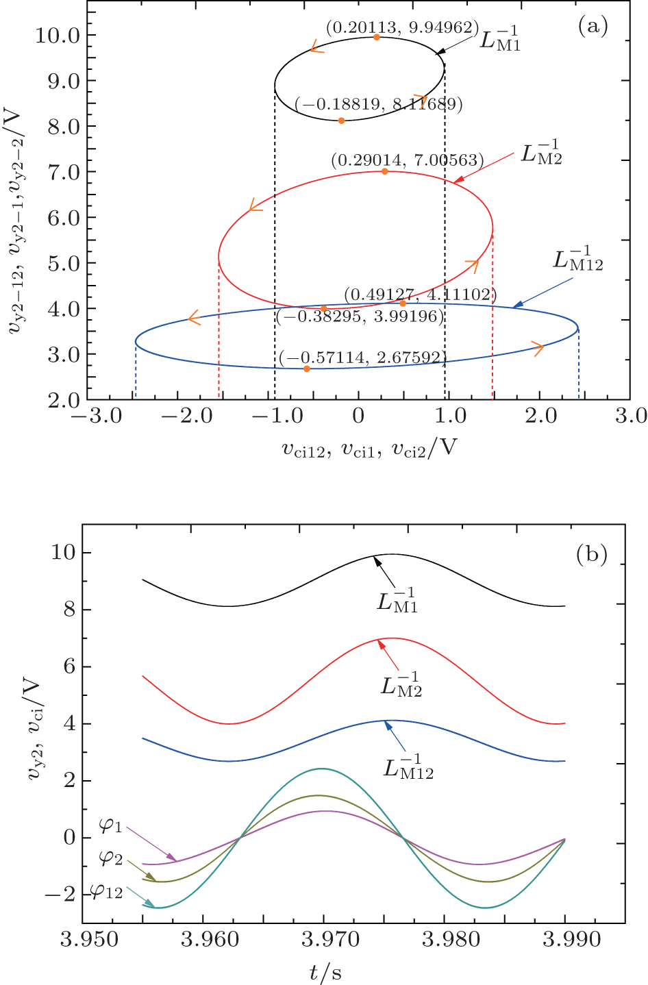 | Fig. 8. Serial ML circuit with identical polarities. (a) Relation between inverse meminductance versus flux; (b) time-domain waveforms of equivalent inverse meminductance and flux. |
Figure 8(b) displays the time-dependent curves of values of equivalent inverse ML and fluxes of this dual ML circuit. Nevertheless, due to the nonlinearity of ML, the flux curves of MLs are no longer sinusoidal waves. These curves imply that the inverse meminductance value of the composite ML is smaller than those of individual MLs, but these three curves approach to their maximum and minimum values simultaneously. This is because two MLs are connected in series with identical polarities, the currents going through each ML are identical. In consequence, as the meminductance of M1 increases, the meminductance of M2 increases, and as the meminductance of M1 decreases, the meminductance of M2 decreases as well.
Figure 8 suggests that corresponding to the alternating input voltage ν 12, equivalent 


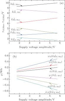
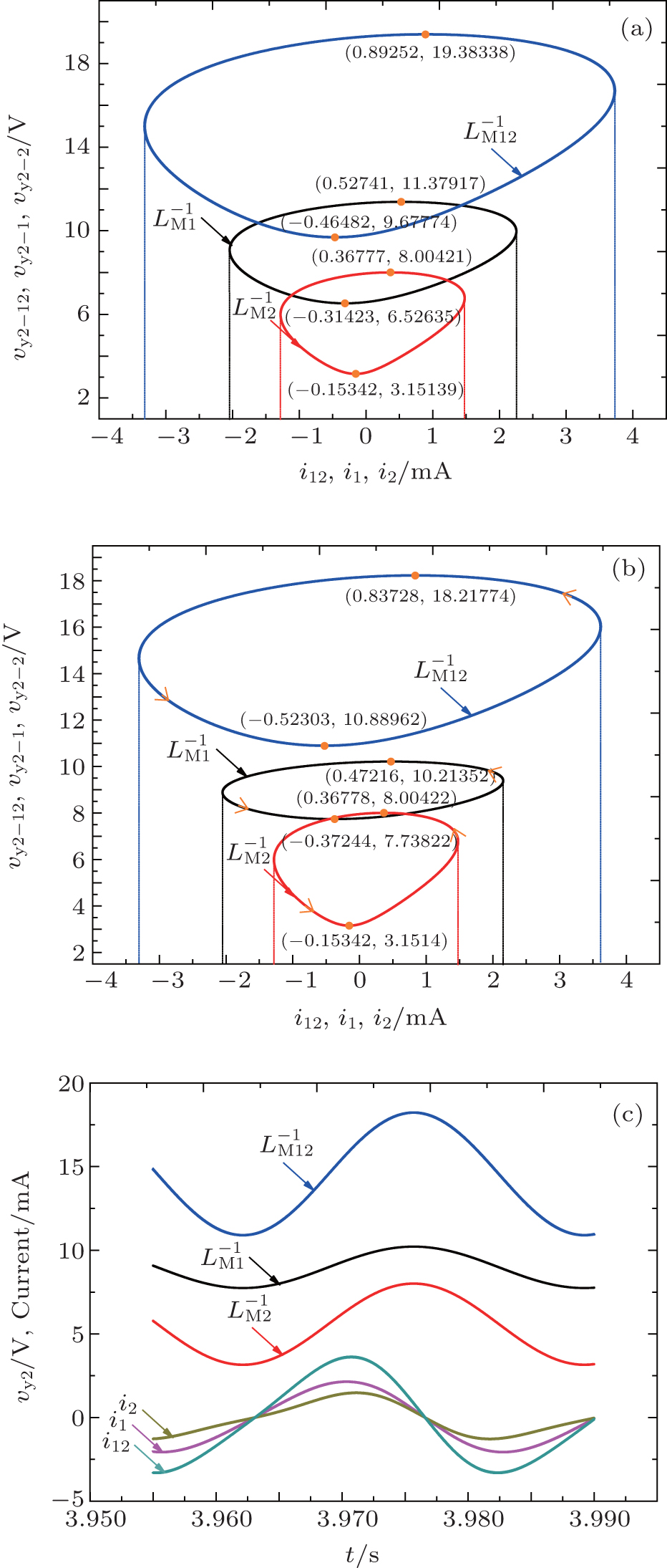
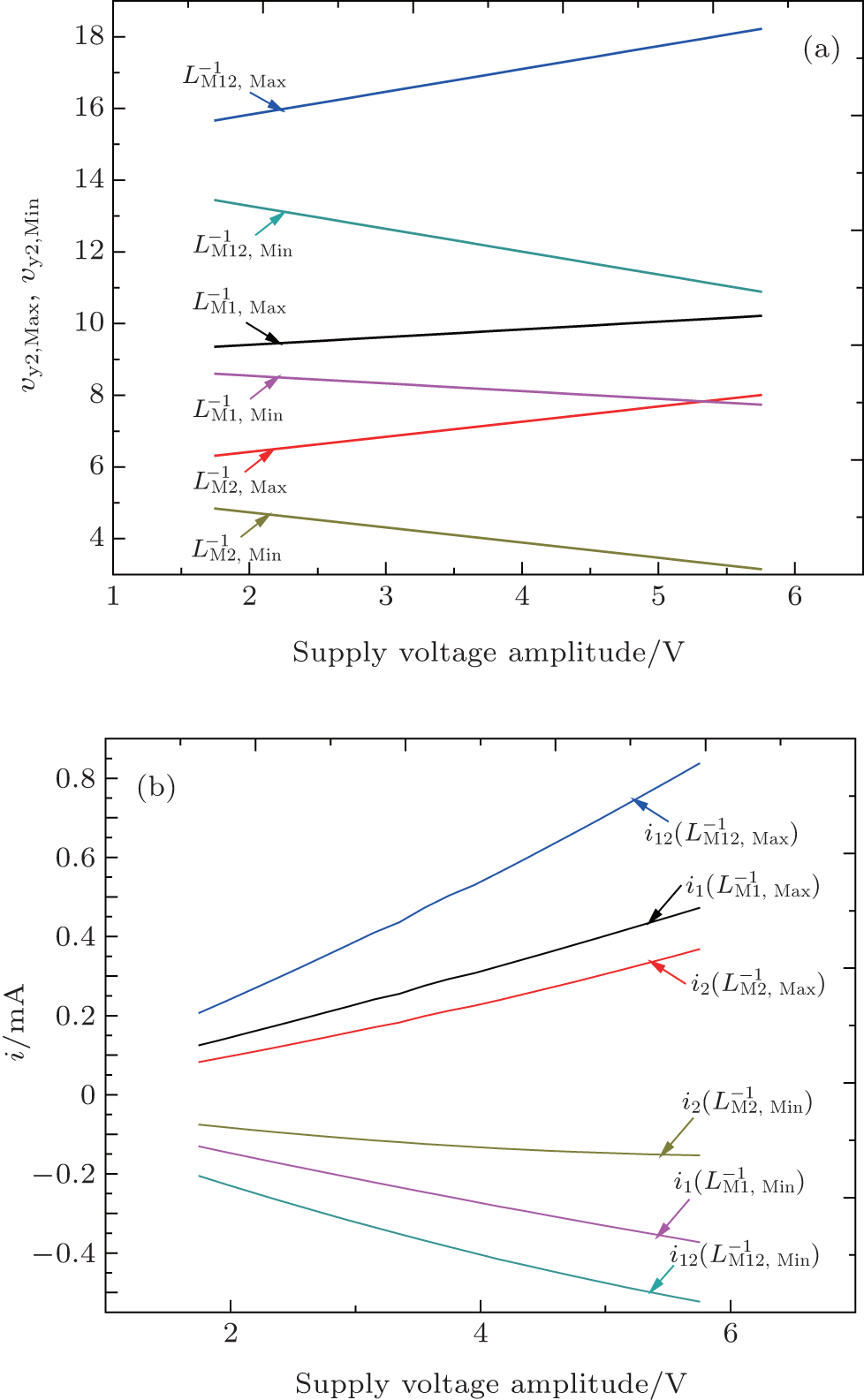
Figure 9 illustrates the variations of the minimum and the maximum equivalent inverse meminductance (ν y2, max and ν y2, min) and the corresponding fluxes φ for each ML and the composite ML with supply voltage amplitude in a range from 1.75 V to 5.75 V in steps of 0.2 V. In Fig. 9(a), when the supply voltage amplitude increases, the maximum values of 


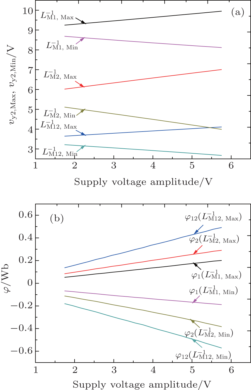 | Fig. 9. (a) Minimum and maximum values of equivalent inverse meminductance vy2, Max and vy2, Min and (b) corresponding fluxes φ for each ML and the composite ML versus supply voltage amplitude in a range from 1.75 V to 5.75 V. |
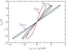
For the connection scenario with opposite polarities, figure 10 presents the curves of current versus fluxes in terms of two individual MLs and the composite ML. Like the case of identical polarities, these two serial MLs also behave together as a new ML with a typical pinched hysteresis loop. According to Eq. (29), the coefficient of ρ for ML2 is a negative value in the opposite connected series, so the curves are slightly different from those in the connection scenario with identical polarities.
 | Fig. 10. Simulation results of pinched hysteresis loops for MLs connected in series with opposite polarities. |
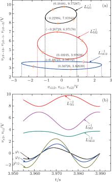
Figure 11 shows the equivalent inverse meminductance, the flux values of each ML, and the composite ML of serially connected MLs with opposite polarities. It can be concluded from Fig. 11(b) that when the curve of 


 | Fig. 11. Serial ML circuit with opposite polarities. (a) Equivalent inverse meminductance versus flux relation, (b) time-dependent waveforms of equivalent inverse meminductance and flux. |
It can be concluded from Fig. 11 that corresponding to the alternating voltage V12, equivalent 


Figure 12 illustrates the variations of the minimum and maximum equivalent inverse meminductance and corresponding fluxes for each ML and the composite ML with supply voltage amplitude in the range from 1.75 V to 5.75 V in steps of 0.2 V. From these curves, we can see that with the increase of the supply voltage amplitude, the maximum values of 


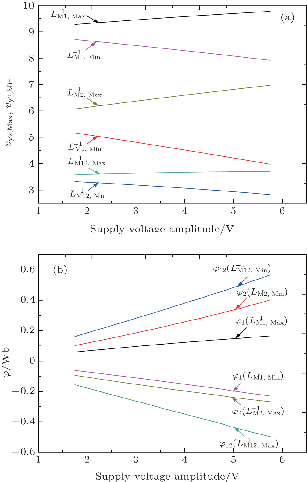 | Fig. 12. Variations of (a) minimum and maximum values of equivalent inverse meminductance and (b) corresponding fluxes for each ML and the composite ML with supply voltage amplitude in the range from 1.75 V to 5.75 V. |
In this case, an inductor of inductance equal to 0.035 H is serially attached to this serial MLs' circuit with identical polarities. In Fig. 14, by only collecting the values of inverse meminductance of two MLs and their corresponding fluxes, we discover that the relation between them leads to a conspicuous conclusion that these two MLs in serial connection also behave like a single ML. That result also validates the good floating performance of this ML based circuit, which renders this composite circuit a wider range of use without grounded restriction.
 | Fig. 13. Simulation results of pinched hysteresis loops for MLs connected in parallel with identical polarities and with another inductor. |
 | Fig. 14. Serial ML circuit with identical polarities connected with an additional inductor. (a) Equivalent inverse meminductance versus flux relation, (b) time-dependent waveforms of equivalent inverse meminductance and flux. |
First, we adopt two scenarios of parameter α to describe the dual MLs in parallel connection, namely, α 1 = α 2 (equal to 235.29412) and α 1 ≠ α 2 (α 1 = 120 and α 2 = 235.29412). The other parameters are β 1 = 0.09 H− 1, β 2 = 0.05625 H− 1, and v12(t) = 5.75sin(73.8π t).
Figure 15 shows the relationships between current and fluxes of two individual MLs and the composite parallel ML circuit, so the slopes of these curves can be used to represent the instant values of equivalent inverse meminductance due to the relation among flux, inductance, and current as L = φ /i. These curves imply that two parallel MLs and their composite ML also possess meminductive characteristics with typical nonlinear pinched hysteresis loops behaving as an inclined “ 8” . According to Eq. (52), the composite meminductance value is smaller than any of the single meminductance values. Thus, the slope of LM12 for a given current is slighter than those of LM1 and LM2.
 | Fig. 15. Simulation results of pinched hysteresis loops for MLs connected in parallel with identical polarities. |
The cases of α 1 = α 2 and α 1 ≠ α 2 for ML circuit connected in parallel with identical polarities are both analyzed. Firstly, coefficient α for two MLs is configured as α 1 = α 2 = 235.29412, and the initial values of the inverse meminductance 

 | Fig. 16. Parallel ML circuit with identical polarities: equivalent inverse meminductance versus current relation (a) α 1 = α 2; (b) α 1 ≠ α 2; (c) time-domain waveforms of equivalent inverse meminductance and current. |
The value of inverse meminductance is in proportion to the value of ρ as described by Eq. (1). For inductors and MLs, the phase difference between voltage and current is π /2, and the current lags π /2 behind the terminal voltage. As a result, the minimum and maximum inverse meminductance values of single ML1, ML2, and ML12 do not occur with the same value of current. If we set different values of coefficient α for two MLs, to be α 1 = 120 and α 2 = 235.29412, there are only slight differences between the maximum and minimum of two ML1 curves. In the following analysis, only the latter scenario of α 1 ≠ α 2 is taken for demonstration.
We can see from Fig. 16(b) that there are two values of the inverse meminductance corresponding to any current, except for the minimum and maximum values. However, due to the nonlinearity of the ML, the maximum and minimum absolute values of current flowing through ML1 and ML2 are different. Evidently, the variation range of current of ML1 is wider than that of ML2. The reason is that in a parallel ML circuit with identical polarities, each single ML has the same terminal voltage. As a result, according to Eq. (1), flux and ρ for each single ML are the same. As β 1 > β 2, the value of 


From Fig. 16(c), we can discover that the equivalent inverse meminductance values of ML1, ML2, and ML12 vary simultaneously in the same time steps, namely, they reach their maximum and minimum values at the same time. Meantime, the value of the instant inverse meminductance of 

By combining Fig. 16(b) with Fig. 16(c), we can conclude that corresponding to the alternating input voltage V12, equivalent 


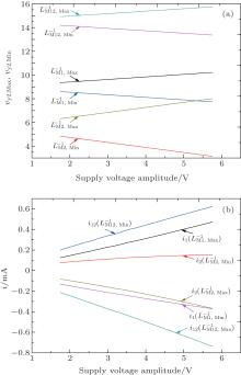
Figures 17(a) and 17(b) illustrate the variations of the minimum and maximum equivalent inverse meminductance and corresponding currents for each ML and the composite ML with the supply voltage amplitude in a range from 1.75 V to 5.75 V, in steps of 0.2 V. We can find from Fig. 17(a) that with the increase of the supply voltage amplitude, the maximum values of 


 | Fig. 17. Variations of (a) the minimum and maximum values of equivalent inverse meminductance and (b) corresponding currents for each ML and the composite ML with supply voltage amplitude. |
Figure 18 shows the relationships between current and flux of two individual MLs and the composite ML with opposite polarities. Like the case of MLs connected in parallel with identical polarities, these two MLs in parallel connection also together behave as a new ML with a typical pinched hysteresis loop. Compared with that in Fig. 15, the variation range of inverse meminductance of the composite ML is smaller than that in the identical scenario.
 | Fig. 18. Simulation results of pinched hysteresis loops for MLs connected in series with opposite polarities. |
Two cases of α 1 = α 2 and α 1 ≠ α 2 are also adopted for analyzing this parallel ML circuit with opposite polarities. Firstly, we set α 1 = α 2 = 235.29412, and the initial values of the inverse meminductance 

 | Fig. 19. Parallel ML circuit with opposite polarities: equivalent inverse meminductance versus current relation (a) when α 1 = α 2; (b) when α 1 ≠ α 2; (c) time-dependent waveforms of equivalent inverse meminductance and current. |
Note that compared with that in Fig. 16(b), the variation range of inverse meminductance of the composite ML is smaller than that in the identical polarity scenario. From Fig. 19(c), we find that equivalent inverse meminductance values of ML1, ML2, and ML12 simultaneously vary, reaching their maximal or minimal values at the same time. However, unlike the identical polarity scenario, the value of the instant inverse meminductance 


The combination of Figs. 19(b) and 19(c) suggests that corresponding to the alternating current i12, equivalent 


Figures 20(a) and 20(b) illustrate the variations of the minimum and maximum equivalent inverse meminductance and corresponding currents for MLs with supply voltage amplitude in the range from 1.75 V to 5.75 V, in steps of 0.2 V. From Fig. 20(a) we can find that with the increase of supply voltage amplitude, the maximum values of 


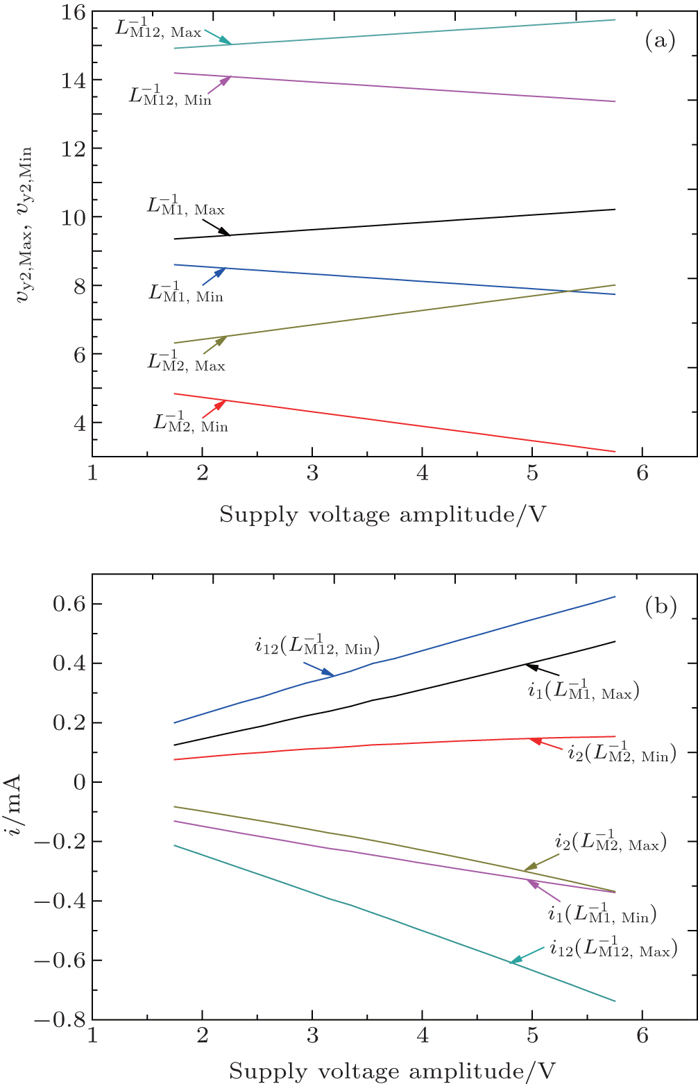 | Fig. 20. Variations of (a) the minimum and maximum values of equivalent inverse meminductance and (b) corresponding currents for each ML and the composite ML with supply voltage amplitude in the range from 1.75 V to 5.75 V. |
In this case, an inductor with an inductance of 0.125 H is serially attached to the ML in parallel connection with identical polarities. In Figs. 21 and 22, we also collect the values of inverse meminductance of two MLs and their corresponding currents, and then find that these two MLs in parallel connection, as connected with an inductor, also behave like one single floating ML.
 | Fig. 21. Simulation results of pinched hysteresis loops for MLs connected in parallel with opposite polarities and with another inductor. |
 | Fig. 22. Parallel ML circuit with identical polarities connected with an additional inductor. (a) Equivalent inverse meminductance versus current relation, (b) time-dependent waveforms of equivalent inverse meminductance and current. |
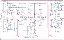
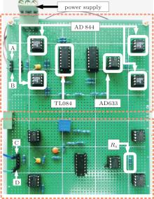
A hardware circuit which can emulate dual MLs is built to validate the correctness of theoretical analysis and simulation results. The experimental data are sampled by an oscilloscope TDS2024C and then processed in the OriginPro 9.0 software to draw experimental curves.
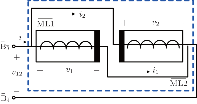
It can be seen from Fig. 6 that four transimpedance operational amplifiers (AD844), two amplifiers (TL084), and one multiplier (AD633) are used to constitute one single ML. As shown in Fig. 23, the circuit enclosed by the upper dotted frame can work as an individual ML emulator (denoted as ML1). Similarly, the circuit enclosed in the lower dotted frame can also work as an individual ML (denoted as ML2). The values of inverse meminductance for each ML can be adjusted via parameters as illustrated in Eq. (64). Experimental results under different circuit configurations can be reached by connecting two MLs together in terms of two polarities. For example, as terminals A and D, B and C are connected together, these two MLs are in parallel connection with opposite polarities.
 | Fig. 23. Hardware circuit connection of dual ML emulators. |
By considering Eqs. (61), (63), and (64), flux φ and inverse meminductance 
The scenarios of MLs in serial connection with identical polarities and parallel connection with opposite polarities are taken for demonstration.
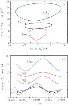
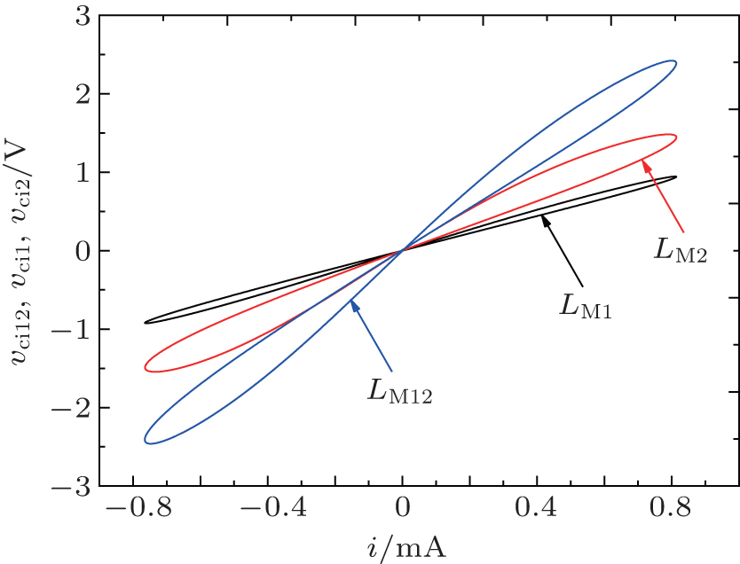
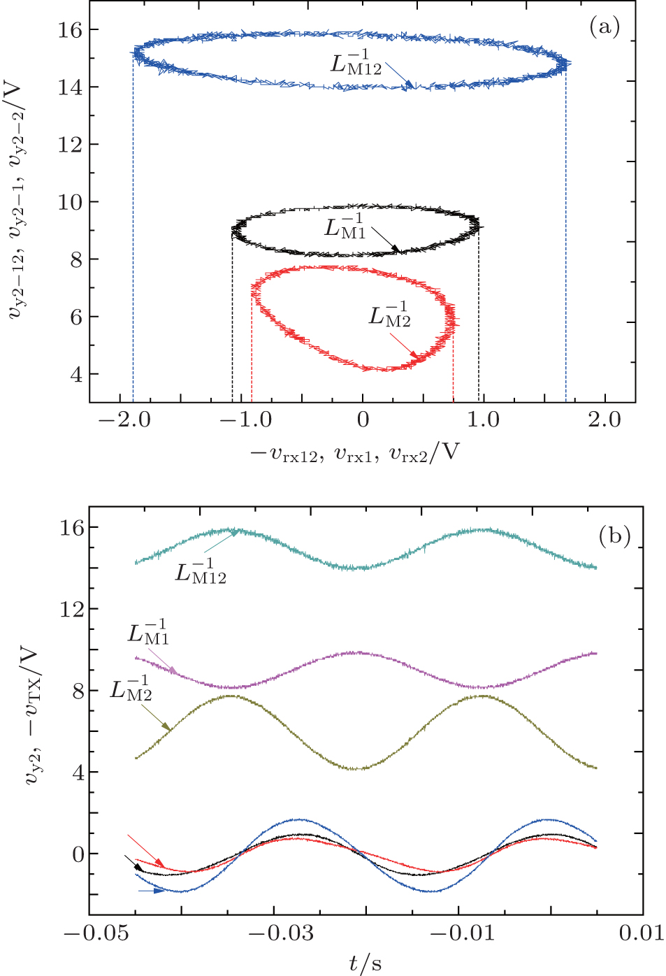
To begin with, the experimental parameters for MLs in serial connection with identical polarities are given as follows: Ri1 = Ri2 = 10 kΩ , Rc1 = Rc2 = 51 kΩ , Ci1 = Ci2 = 1 u, C11 = C12 = 0.1 u, R11 = R12 = 51 kΩ , R21 = R22 = 200 kΩ , R31 = R32 = 25 kΩ , R41 = 50 kΩ , R42 = 80 kΩ , R51 = R52 = 30 kΩ , R61 = R62 = 51 kΩ , Rx1 = Rx2 = 1 kΩ , vs1 = vs2 = − 15 V. Based on these parameters, the initial values of inverse meminductance of two MLs are calculated to be β 1 = 0.09 H− 1 and β 2 = 0.05625 H− 1. Meanwhile, the values of α 1 and α 2 are configured as α 1 = α 2 = 235.29412. As for the supply voltage v12, it can be described by a 36.9 Hz sinusoidal function with 5.75 V amplitude. Experimental data of equivalent flux and inverse meminductance for serial ML circuit with identical polarities are collected and shown in Fig. 24. Obviously, the experimental loops are in close proximity to the simulated results in Fig. 8.
 | Fig. 24. Measured curves of serial ML circuit with identical polarities: (a) relation between inverse meminductance versus flux; (b) time-dependent waveforms of equivalent inverse meminductance and flux. |
The parameters for experimentally testing MLs in parallel connection with opposite polarities are then configured as follows: Ri1 = Ri2 = 10 kΩ , Rc1 = Rc2 = 51 kΩ , Ci1 = Ci2 = 1 u, C11 = C12 = 0.1 u, R11 = 100 kΩ , R12 = 51 kΩ , R21 = R22 = 200 kΩ , R31 = R32 = 25 kΩ , R41 = 50 kΩ , R42 = 80 kΩ , R51 = R52 = 30 kΩ , R61 = R62 = 51 kΩ , Rx1 = Rx2 = 1 kΩ , vs1 = vs2 = − 15 V. Thus, the parameters in Eqs. (8) and (9) are configured as β 1 = 0.09 H− 1, β 2 = 0.05625 H− 1, α 1 = 120, and α 2 = 235.29412. The supply voltage v12 is described by v12(t) = 5.75sin(73.8π t). Experimental data of equivalent current and inverse meminductance for parallel ML circuit with opposite polarities are gathered and plotted in Fig. 25, which is highly consistent with the preceding waveform in Fig. 19.
 | Fig. 25. Measured curves of a parallel ML circuit with opposite polarities: (a) equivalent inverse meminductance versus current relation, and (b) time-dependent waveforms of equivalent inverse meminductance and current. |
However, there remain some minimal errors between simulated results and experimental measured results. For example, the time-domain curve of 

In this paper, the composite behaviors of serial and parallel ML circuits with different polarities are theoretically analyzed, then simulated based on PSPICE, and finally characterized by the hardware circuit. The simulation and hardware results are in good accordance with the theoretical analysis. Despite the connection properties, the composite ML also acts like another time-integral-of-flux controlled ML with new meminductance, and different connections in terms of topologies and polarities can finally lead to various kinds of inverse meminductance values. Additionally, the floating performance of the composite ML circuit is also validated, which renders the circuit of composite dual MLs a wider scope of application without grounded restriction. The above characteristics provide unique approaches for MLs to be utilized in circuit designs. The main contribution of this work is that it provides some practicable conclusions about composite MLs connections and the analyzing method can be extended to multiple MLs connection and be instructive to subsequent research work on the potential applications of ML.
| 1 |
|
| 2 |
|
| 3 |
|
| 4 |
|
| 5 |
|
| 6 |
|
| 7 |
|
| 8 |
|
| 9 |
|
| 10 |
|
| 11 |
|
| 12 |
|
| 13 |
|
| 14 |
|
| 15 |
|
| 16 |
|
| 17 |
|
| 18 |
|
| 19 |
|
| 20 |
|
| 21 |
|
| 22 |
|