


Magnetic–optical bifunctional CoPt3/Co multilayered nanowire arrays
[Su Yi-Kuna) , Yan Zhi-Longa) , Wu Xi-Minga) , Liu Huana) , Ren Xiaob) , Yang Hai-Tao†b)  ]
]
]
|
|


†Corresponding author. E-mail: htyang@iphy.ac.cn
*Project supported by the National Natural Science Foundation of China (Grant Nos. 51472165, 51471185, and 11274370).
CoPt3/Co multilayered nanowire (NW) arrays are synthesized by pulsed electrodeposition into nanoporous anodic aluminum oxide (AAO) templates. The electrochemistry deposition parameters are determined by cyclic voltammetry to realize the well control of the ratio of Co to Pt and the length of every segment. The x-ray diffraction (XRD) patterns show that both Co and CoPt3 NWs exhibit face-centered cubic ( fcc) structures. In the UV-visible absorption spectra, CoPt3/Co NW arrays show a red-shift with respect to pure CoPt3NWs. Compared with the pure Co nanowire arrays, the CoPt3/Co multilayered nanowire arrays show a weak shape anisotropy and well-modulated magnetic properties. CoPt3/Co multilayered nanowires are highly encouraging that new families of bimetallic nanosystems may be developed to meet the needs of nanomaterials in emerging multifunctional nanotechnologies.
Multilayered nanowires (NWs) with controlled structure and interface interactions can exhibit novel physical and chemical properties that will be necessary for future technological applications. Multilayered NWs consisting of alternating ferromagnetic (FM) and nonmagnetic metallic layers have become a hot research topic in recent years, such as Co/Pt, [1] Co/Au, [2] NiCoCu/Cu, [3] CoPt/Pt, [4] Co(Cu)/Cu, [5] NiFe/Pt, [6] etc. The magnetic properties of NWs can be adjusted through changing the relative thickness of nonmagnetic metallic layer. Compared with single-component counterparts, multilayered NWs with different material components can also exhibit multifunctionality. For instance, Fe– Au barcode NWs have been explored for their magnetic and optical properties.[7] A synthetic hybrid nanomotor consisting of multisegment Pt– Au– Ag– Ni NWs can combine chemically powered propulsion and magnetically driven locomotion.[8] The ferromagnetism of Co/Pt barcodes can be enhanced through interfacial alloying processes via a thermally induced phase transition.[9] NWs with a ferromagnetic metal alternated with a nonmagnetic metal can also exhibit giant magnetoresistance and are proposed as nanosensors.[10]
There are many researches about the optical properties of pure metal NWs, such as Au, [11] Ag, [12] and Pt[13] NWs. But the optical property of metal alloy NWs has received less attention at present.[12] Therefore, in the present paper, multilayered NWs consisting of alloy CoPt3 segments with weak FM properties (WFM) and FM Co segments are prepared by pulsed electrodeposition inside nanoporous anodic aluminum oxide (AAO) templates, and their optical and magnetic properties are investigated by UV-vis spectrophotometer and superconducting quantum inference device magnetometer (SQUID, MPMS XL), respectively. The bifunctions of magnetic and optical properties in the multilayered NWs are targeted for the separation, detection, and transport of biomedical materials.[14]
The AAO templates used in our experiments were purchased from Whatman Company (200-nm nominal pore diameter and 60-μ m thickness). The crystal structure was determined by x-ray diffraction (D8-X, Bruker, Germany) with Cu kα radiation (λ = 1.5418 Å ; 40 kV × 300 mA). The absorption spectrum and hysteresis loop of CoPt3/Co NW arrays/AAO template were measured by UV-vis spectrophotometer and VSM. The morphology of the samples wass characterized by scanning electron microscopy (SEM, Hitachi SU-70). To separate the NWs from the template for SEM observation, the sample was immersed into acid solution (3.5 vol% H2CrO4 + 40 g/L H3PO4) for 10 h at 70 ° C to remove alumina. As-obtained product was washed thoroughly with deionized water, and then centrifuged several times. Afterwards, a drop of suspension was placed on a silicon wafer for SEM examination. A Chi660D Electrochemical Station (Cordava) was used for both the cyclic voltammetric measurement and the bamboo-shape CoPt3/Co pulse deposition in a three-electrode cell. Before the electrodeposition, a layer of Ag has been evaporated on one side of the AAO template. The Ag-coated AAO template and a piece of Pt plate were used as working and counter electrodes, respectively. A saturated calomel electrode (SCE) was utilized as a reference. The electrolyte solution consisting of 2-M CoSO4, 0.00375-M H2PtCl6, and 0.5-M H3BO3 was employed to deposit CoPt3/Co NWs. The deposition potential was alternately switched from – 1 V (vs. SCE) for 10 s to – 0.3 V (vs. SCE) for 10 s to obtain Co and CoPt3 segments, respectively. The deposition was carried out at room temperature.
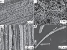
The morphology of as-grown NWs arrays has been measured by scanning electron microscopy (SEM). Figure 1(a) shows a cross-sectional SEM image of Co NW arrays in an AAO template. The NWs are parallel to each other and the lengths of the NWs are also very uniform. Figure 1(b) shows the low-resolution SEM image of CoPt3 NWs released from AAO template. When the top alumina of the AAO template was dissolved away, the NWs embedded in the template were released gradually and inclined to agglutinate together. The sample still consists of a large quantity of straight NWs. Some wires bend together, which may be due to internal stress during electro-deposition. Figure 1(c) shows the TEM image of CoPt3/Co NWs in AAO template prepared by electro-deposition for 0.5 h. Compared with Co and CoPt3 NWs, the CoPt3/Co NWs display a clearly bamboo-shape multilayered structure. After being released from AAO template, the NWs (as shown in Fig. 1(d)) contain two segments and the thickness values of Co and CoPt3 segment are 50 nm and 10 nm, respectively. The diameter of Co segment shows a slight shrink because Co is easier to dissolve in acid solution than CoPt3 alloy. All the diameters of as-deposited NWs are around 200 nm, which is well consistent with the pore diameter of the used AAO template.
 | Fig. 1. SEM images of (a) Co NWs, (b) CoPt3 NWs, CoPt3/Co NWs with 50-nm thick CoPt3 layers and 10-nm thick Co layers (c) in AAO template, and (d) after dissolution from AAO template. |
To reveal the control mechanism on the atom ratio of CoPt3 alloy and the length of Co and CoPt3 segments, the cyclic voltammogram is investigated during electrodeposition of Co and Pt electrolyte solution. As shown in Fig. 2(a), the scan started from – 1.0 V to 1.0 V, and then reversely to – 1.0 V with a scan rate 0.05 V/S. The peak at about 0.03 V is attributed to the Co deposition from Co2+ . The reduction peak of Pt is not founded because of the low concentration of chloroplatinic acid. Compared with the reduction peak of Co2+ in the deposition of pure Co NWs, the reduction peak in the deposition of CoPt3/Co NWs shows a shift from – 0.2 V, which is due to the influence of Pt cation in electrolyte solution. The majority of the deposition was Co after a positive deposition potential had been chosen because the concentration of Co2+ was 500 times higher than that of 
 | Fig. 2. (a) Cyclic voltammogram of deposition of CoPt3/Co NWs, Co NWs, and Pt NWs in a bath containing 2-M CoSO4 + 0.00375-M H2PtCl6 + 0.5-M H3BO3, containing 0.00375-M H2PtCl6 + 0.5-M H3BO3, and containing 2-M CoSO4 + 0.5-M H3BO3, respectively, scan rate = 50 mV/s; (b) the influence of deposition potential on Co– Pt atomic ratio. |
Figure 3 exhibits the XRD patterns CoPt3/Co, Co, and CoPt3 NWs, respectively. The diffraction peaks centered at 40.3° , 46.9° , and 68.2° were found in both CoPt3/Co and CoPt3 NWs, which can be indexed to (111), (200), and (220) planes of f cc CoPt3 (JPDF#-29-0499). The XRD pattern also shows the presence of asymmetric peaks (200) and (220) around 46.9° and 68.2° , which are attributed to lattice defects resulting from the faster deposition rate. The peaks located at 41.9° , 44.6° , and 76.1° are indexed to the (111), (200), and (220) plane of pure Co (JPDF#-01-1255). Neither the crystalline orientation of Co segment nor the crystalline orientation of CoPt3 segment is observed since the aspect ratio is less than 1. The comparison between XRD patterns of Co and CoPt3 NWs deposited by the same method, clearly reveals that the NWs contain two different structures of Co and CoPt3 alloy.[15]
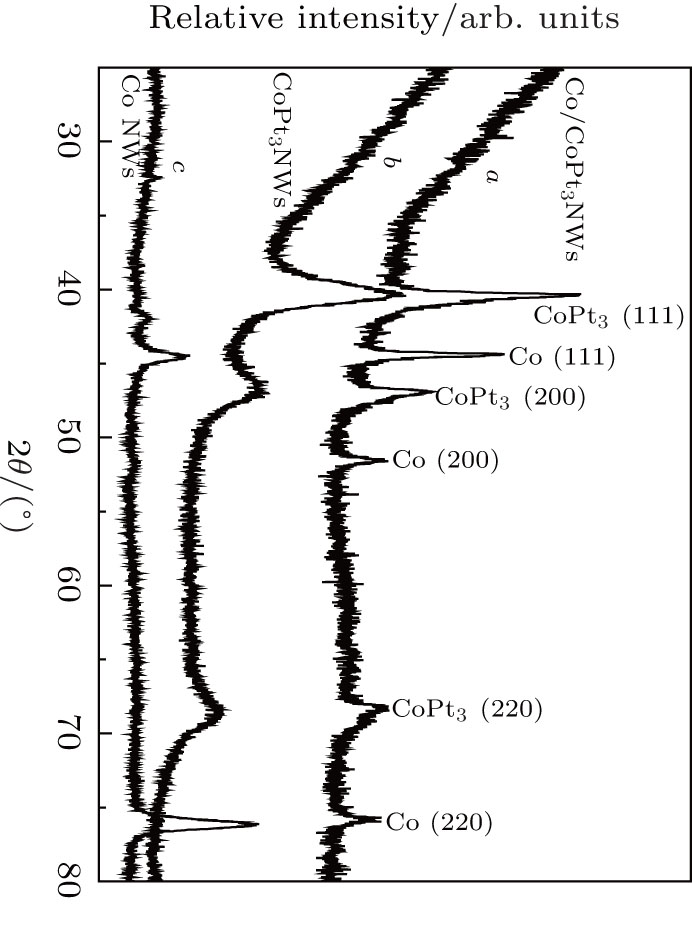 | Fig. 3. X-ray diffraction patterns of (curve a) CoPt3/Co NWs, (curve b) CoPt3 NWs, and (curve c) Co NWs. |
The UV-vis diffuse reflectance spectra of CoPt3 and CoPt3/Co NWs are shown in Fig. 4. CoPt3 NWs show two weak resonances peaked at 260 nm and a strong and broad peak at 622 nm, respectively. While CoPt3/Co NWs show two weak resonances peaked at 284 nm and a strong and broad peak at 645 nm, respectively. Generally, Pt nanoparticles (NPs) and NWs dispersed in solution are reported to show a very weak resonances peaked below 450 nm, [16, 17] or no resonances peaked between 200 nm and 800 nm due to a very small imaginary part of its dielectric constant.[18, 19] And Co NPs are not usually observed to have any resonances peaked in the UV-vis region. As is well known, two distinct surface plasmon resonances are generated by the anisotropy of the nanowires. One response is parallel to the short axis (transverse) and the other is parallel to the long axis (longitudinal). So the resonances of CoPt3 NWs peaked at 260 nm and 622 nm are corresponding to the transverse and longitudinal modes respectively. In the case of Co/CoPt3 NWs, Co segments bridge the gap between the CoPt3 segments and contribute to the plasmonic behavior without disrupting the original resonance structure.[16] But the positions of the other two absorption bands present a distinctive red-shift of more than 20 nm, which indicates that free electrons in the Co segment actively participate in the plasmon excitations in the CoPt3 segment. Electron transfer out between two segments leads to the occurrence of red-shift.[19] The coupling optic properties of CoPt3/Co NWs can be used in light detection and catalysis in the UV-vis light range.
 | Fig. 4. UV-vis spectra of nanowires arrays/AAO template composite (curve a) CoPt3/Co NWs and (curve b) CoPt3 NWs. |
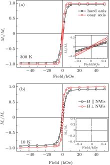
Figure 5 shows the 10-K and 300-K hysteresis loops of CoPt3/Co NWs with external field parallel (‖ ) and perpendicular (⊥ ) to the axes of the NWs. The magnetization is normalized by devising the saturation magnetization at 10 K and 300 K. At 300 K, the coercivity and remanence are small when the applied field is parallel (Hc = 70 Oe, Mr = 0.015) and perpendicular (Hc = 50 Oe, Mr = 0.02) to the nanowires (1 Oe = 79.5775 A· m− 1). At 10 K, the coercivity and remanence values increase to Hc = 300 Oe, Mr = 0.06 for the case of H ‖ NWs, and Hc = 240 Oe, Mr = 0.12 for the case of H⊥ NWs. The magnetic behavior indicates that CoPt3/Co NWs is a typical soft-ferromagnetic material and its easy axis is perpendicular to the nanowire axis at both 10 K and 300 K according to the shapes of the loops of CoPt3/Co NWs. The aspect ratio of Co segment in the as-prepared CoPt3/Co NWs is only 0.25, which results in the low anisotropy energy of Co segments along the NW axis since the Pt-rich CoPt3 segment inhibits domain wall motion and exchange interaction among Co grains. Unlike long magnetic NWs with a large aspect ratio (such as pure Co NWs prepared in AAO template, much larger than 1) in which the easy magnetization direction is parallel to the NW axis and the magnetism is usually dominated by shape anisotropy, [20] the FM/WFM multilayered NWs are usually dominated by crystalline anisotropy and offer much flexibility in tailoring the magnetism of NWs by taking advantage of the easy control of the thickness values of FM layers.[9]
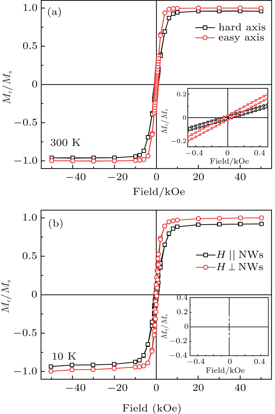 | Fig. 5. 10-K and 300-K hysteresis loops of CoPt3/Co NWs arrays with different applied field directions. |
In summary, we have fabricated multilayered bifunctional CoPt3/Co NW arrays by pulsed electrodeposition into AAO templates. The well-defined layered nanostructure of CoPt3/Co NWs is confirmed through the structural and morphology analysis. Both Co and CoPt3 segments exhibit f cc structures and well-controlled length. Such a multilayered nanostructure reveals the different magnetic and optical properties that are beyond those of the individual components as a result of coupling of the optical sensing elements with the magnetic actuator. The heterojunction bifunctional NWs may evolve as useful nanoscale building blocks for magnetic-optical devices and as magnetic-relative catalysis application. The relation between desired physical properties and optimum structure, such as dimension needs further studying. So our studies are highly encouraging that new families of bimetallic nanosystems may be developed to meet the needs of emerging multifunctional technologies, where there is a continuous drive to find nanomaterials with ever more exotic optic, magnetic, and other properties, and where the assembly of these fundamental building blocks can lead to new types of functionalities.
| 1 |
|
| 2 |
|
| 3 |
|
| 4 |
|
| 5 |
|
| 6 |
|
| 7 |
|
| 8 |
|
| 9 |
|
| 10 |
|
| 11 |
|
| 12 |
|
| 13 |
|
| 14 |
|
| 15 |
|
| 16 |
|
| 17 |
|
| 18 |
|
| 19 |
|
| 20 |
|
| 21 |
|