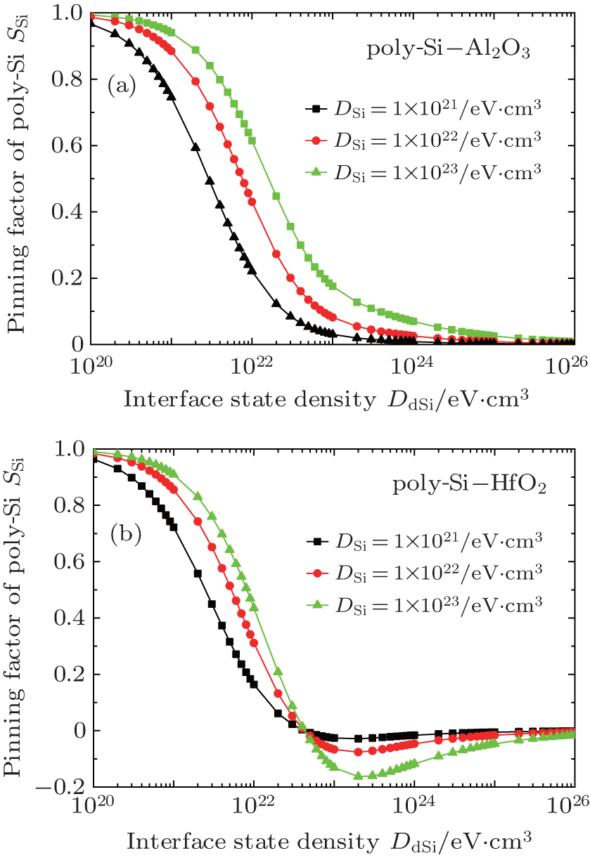
Fermi level pinning effects at gate–dielectric interfaces influenced by interface state densities

Fermi level pinning effects at gate–dielectric interfaces influenced by interface state densities |
| (a) Plots of semiconductor pinning factor S Si for ploycrystalline silicon–Al2O3 versus interface state density D dSi with various values of D Si. The large D dSi enables S Si to be pinned at 0. (b) Plots of pinning factor of poly-Si S Si versus interface state density D dSi. S Si for ploycrystalline silicon–HfO2 become negative with the large D dSi. |
 |