


Dynamics and stabilization of peak current-mode controlled buck converter with constant current load
[Leng Min-Rui, Zhou Guo-Hua† , Zhang Kai-Tun, Li Zhen-Hua]
, Zhang Kai-Tun, Li Zhen-Hua]
|
|


†Corresponding author. E-mail: ghzhou-swjtu@163.com
*Project supported by the National Natural Science Foundation of China (Grant No. 61371033), the Fok Ying-Tung Education Foundation for Young Teachers in the Higher Education Institutions of China (Grant No. 142027), the Sichuan Provincial Youth Science and Technology Fund, China (Grant Nos. 2014JQ0015 and 2013JQ0033), and the Fundamental Research Funds for the Central Universities, China (Grant No. SWJTU11CX029).
The discrete iterative map model of peak current-mode controlled buck converter with constant current load (CCL), containing the output voltage feedback and ramp compensation, is established in this paper. Based on this model the complex dynamics of this converter is investigated by analyzing bifurcation diagrams and the Lyapunov exponent spectrum. The effects of ramp compensation and output voltage feedback on the stability of the converter are investigated. Experimental results verify the simulation and theoretical analysis. The stability boundary and chaos boundary are obtained under the theoretical conditions of period-doubling bifurcation and border collision. It is found that there are four operation regions in the peak current-mode controlled buck converter with CCL due to period-doubling bifurcation and border-collision bifurcation. Research results indicate that ramp compensation can extend the stable operation range and transfer the operating mode, and output voltage feedback can eventually eliminate the coexisting fast-slow scale instability.
Complex dynamics and nonlinear phenomenon, including low-frequency oscillation, [1, 2] period-doubling bifurcation, [3, 4] Hopf bifurcation, [5, 6] border collision bifurcation and chaos, [7– 12] exist extensively in switching DC-DC converters which can be regarded as nonlinear time-varying systems, and have a great influence on their performance. Therefore, it is of great significance in both theoretical research and engineering application to investigate the nonlinear phenomenon and the way to stabilize the converters.
The current-mode controlled converters have been widely studied and used due to their fast responses to input variation and easy-to-limit currents.[13] Recently, the dynamical behaviors of current-mode controlled converters with resistive load have been reported by establishing discrete iterative map models and cycle-by-cycle simulation.[14, 15] The period-doubling bifurcation and border collision in the second-order switching converter were revealed, which is meaningful for dynamics analysis.[16] For the sake of making converters in stable operation, adding ramp compensation to the feedback control circuit is an efficient way which has received increasing attention. Based on the piece-wise smooth model of the switching converter, the equations of state transition were derived and the dynamics with ramp compensation were studied.[17] The normalized mapping models of switching converters with ramp compensation were also established in order to illustrate the existence of three operation regions in parameter space.[18, 19] It was reported that the ramp compensation has an influence on the stabilities and operation-mode shifts of converters.[20] Currently, lots of researches have been carried out on converters with ramp compensation where the output voltage is considered as a constant voltage source, [17– 19] which can reduce the second-order system to the first-order system, however less attention is paid to the second-order converters with ramp compensation relatively and the influence of voltage feedback loop on their stabilities is ignored.
Switching DC-DC converters with constant current load (CCL) have a potential application in lighting emitting diode (LED), becoming an important research topic.[21, 22] At present, there are a few researches of switching converters with CCL. The unique fast-slow scale instability under current-mode control without output voltage feedback is investigated in the converter with CCL[23, 24] and verified theoretically by the eigenvalues of the Jacobian, [25] without discussing the stabilization or stable control of them.
In this paper, we take the peak current-mode controlled buck converter with CCL as a research object, adding ramp compensation and output voltage feedback to the converter, deducing the piece-wise smooth model and discrete iterative map model with two borders, exploring the complex dynamics of this converter and how the slope of ramp compensation and the proportional coefficient of outer voltage loop affect the stabilities.
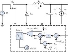
A peak current-mode controlled buck converter with CCL is shown in Fig. 1, where the buck converter consists of an input voltage source E, a CCL Io, a switch ST, a diode SD, an inductor L, and a capacitor C. The peak current-mode controller contains an inner current loop and an outer voltage loop, where the control pulse is obtained by comparing the inductor current iL with reference current iref, which is composed of a constant current Iref, a ramp compensation current, and the output voltage feedback. To maintain the order of the system, an error amplifier with the proportional component is considered in the output voltage feedback loop, where k is the proportional coefficient.
 | Fig. 1. Buck converter with CCL under peak current-mode control. |
The operation principle of the system can be briefly described as follows. The flip– flop latch is set at the beginning of each switching cycle by the clock signal and the switch ST is turned on. When the inductor current iL increases linearly to the reference current iref, the switch ST is turned off and the inductor current falls linearly until the end of the current switching cycle. If the inductor current iL drops and remains zero during the off state of ST, the converter operates in discontinuous conduction mode (DCM), otherwise in continuous conduction mode (CCM).
There are three switch operation states in the peak current-mode controlled buck converter with CCL. The dynamic equations can be obtained by defining the iL and vC as state variables.
In state 1, ST is on and SD is off. The dynamic equations are derived as follows:


In state 2, ST is off and SD is on. The equations are given as follows:


In state 3, ST is off and SD is off. The equations are given as follows:


It contains the first two states when the converter operates in CCM, while in DCM, states 1– 3 are involved and repeated periodically. From the dynamic equations of the converter we can see that the system is nonlinear and piecewise smooth, which makes it difficult to investigate the dynamics of the converter directly. By sampling synchronously for the inductor current and capacitor voltage at the beginning of each switching cycle, the discrete iterative map model can be derived.
The values of inductor current and capacitor voltage at the beginning of the n-th cycle and (n + 1)-th cycle are assumed to be in, vn, in+ 1, and vn+ 1, respectively. With the variation of circuit parameters, two borders Ib1 and Ib2 of the inductor current are defined in discrete state-space, as shown in Fig. 2. When in = Ib1 and in+ 1 = iref, it is shown in Fig. 2(a) that the switch ST is on during the whole period, indicating that the inductor current remains increasing. When in = Ib2 and in+ 1 = 0, figure 2(b) reveals that the inductor current rises at first and falls to zero at the end of the period due to the off-time td.
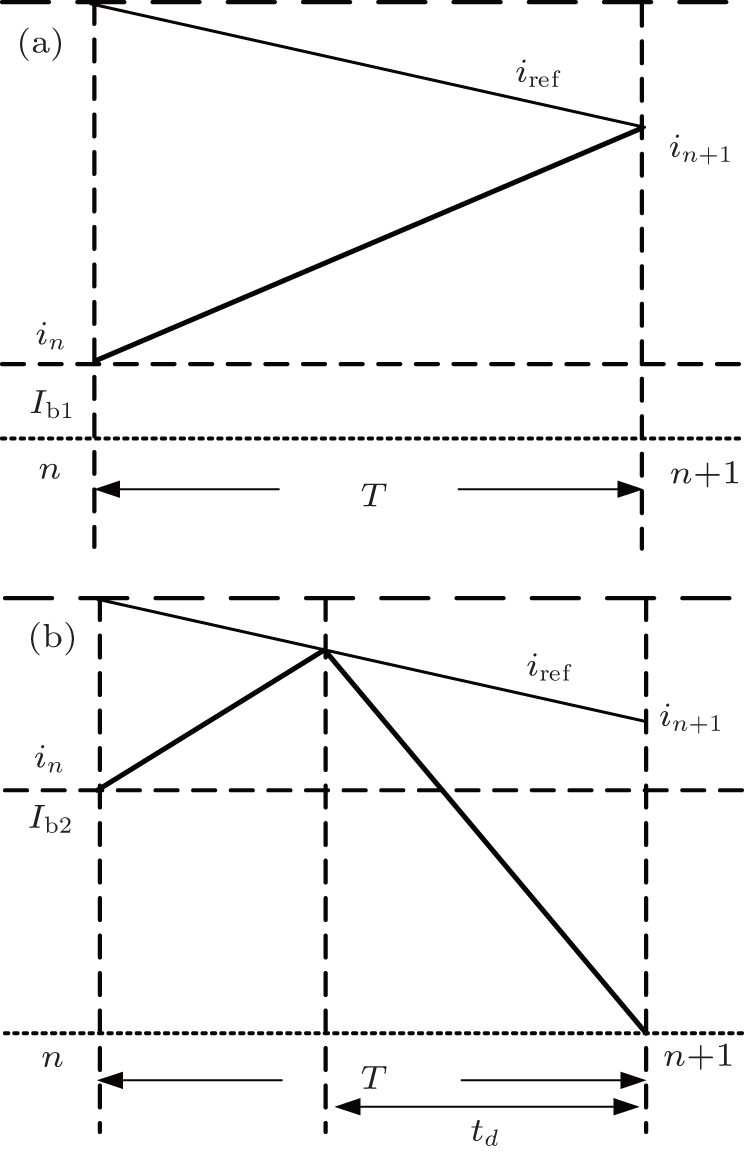 | Fig. 2. Two boundaries of inductor current: (a) in = Ib1, in+ 1 = iref; (b) in = Ib2, in+ 1 = 0. |
The two borders of the inductor current can be solved approximately from Fig. 2 and Eqs. (1)– (6) as follows:


where T is the switching period and iref is given by

Here, mc is the slope of the ramp compensation current and Vref is the reference voltage.
If in ≤ Ib1, the switch ST keeps the on-state throughout the switching cycle and the converter just operates in state 1. The stroboscopic map can be written as follows:


where 
If Ib1 ≤ in ≤ Ib2, the converter operates in state 1 and state 2 within one switching cycle. After the on-time interval tn of the switch ST, the inductor current iL rises to iref, and then ST is turned off until the end of the switching cycle. The iterative map is described by


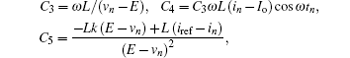
where tn = ((iref − in)L)/(E − vn), vc (tn) = (vn − E)cos ω tn + ω L(in − Io)sin ω tn + E, c1 = iref − Io, and c2 = − vc (tn)/ω L.
If Ib2 ≤ in, the inductor current will rise at the beginning and drop to zero before the end of the switching cycle. The iterative map is given as


where

and td = Liref/vc(tn)
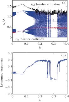
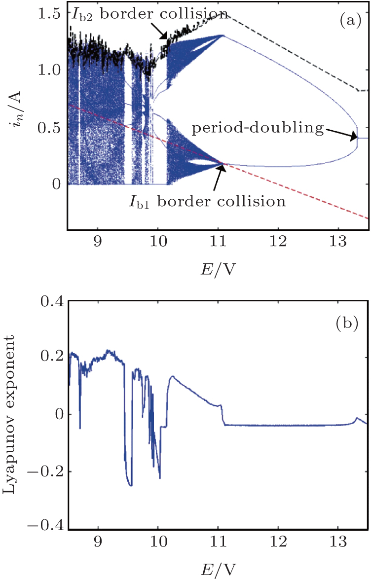
Bifurcation behaviors of peak current-mode controlled buck converter with CCL can be analyzed with the change of circuit parameters on the basis of a discrete iterative map model. The current load Io and input voltage source E have important influences on the performance of the converter, each of which should be taken as a bifurcation parameter. Adopting circuit parameters k = 0.2, E = 9.6 V, Iref = 1.2 A, Vref = 6 V, C = 100 μ F, L = 250 μ H, mc = 0 and T = 50 μ s, and taking Io as the bifurcation parameter which varies from 0.5A to 1.3A, the bifurcation diagram of the inductor current is demonstrated in Fig. 3(a) and the corresponding Lyapunov exponent spectrum is shown in Fig. 3(b).
 | Fig. 3. (a) Bifurcation diagram and (b) Lyapunov exponent spectrum varying with Io. |
As can be seen from Fig. 3, the orbit of the converter is transferred from steady period-1 state to subharmonic oscillation (period-2 state) with the decreasing of Io due to period-doubling bifurcation at Io = 1.024 A, in the meanwhile the corresponding Lyapunov exponent goes up from negative to zero. Border collision appears at Io = 0.965 A when the inductor current reaches the border Ib1, while the Lyapunov exponent rises from a negative value to a positive value, making the converter present in a robust and chaotic state, which can be called CCM robust chaos. For the further decreasing of Io, the inductor current reaches border Ib2 around Io = 0.833 A, and multiple periodic windows emerge from the bifurcation diagram and manifest weak chaos, which can be called DCM weak chaos. The corresponding Lyapunov exponent varies between a negative value and a positive value alternatively due to the existence of some multiple periodic windows. From the analysis above, it is shown that the converter operates in CCM robust chaos in a range of Io = 0.833 A– 0.965 A, and operates in DCM weak chaos in a range of Io = 0.5 A– 0.833 A.
The above analysis method can also be used in the case where E is taken as the bifurcation parameter. By fixing Io = 0.74 A, the inductor current bifurcation diagram can be obtained and shown in Fig. 4(a) with E changing from 8.5 V to 13.5 V, and its Lyapunov exponent is displayed in Fig. 4(b).
 | Fig. 4. (a) Bifurcation diagram and (b) Lyapunov exponent spectrum varying with E. |
When the input voltage source E is reduced eventually to 13.32 V, the converter is driven to operate in subharmonic oscillation via losing steady period-1 state due to perioddoubling bifurcation. As E decreases approximately to 11.1 V, the converter enters into CCM robust chaos due to the border collision with the border Ib1. The buck converter with CCL exhibits weak chaos in DCM when the border collision with border Ib2 takes place at E = 10.09 V. The corresponding Lyapunov exponent is consistent with the bifurcation diagram, illustrating the same dynamical behaviors for a certain range of E.
The ramp compensation and output voltage feedback have obvious influences on the stability of the peak current-mode controlled buck converter with CCL. Based on discrete iterative map model, dynamical behaviors with different slopes of ramp compensation can be analyzed to explore the effect of the ramp compensation on the stabilization of the converter. Taking Io as a bifurcation parameter, the bifurcation diagram under mc = 1000 and mc = 6000 can be acquired and shown in Fig. 5.
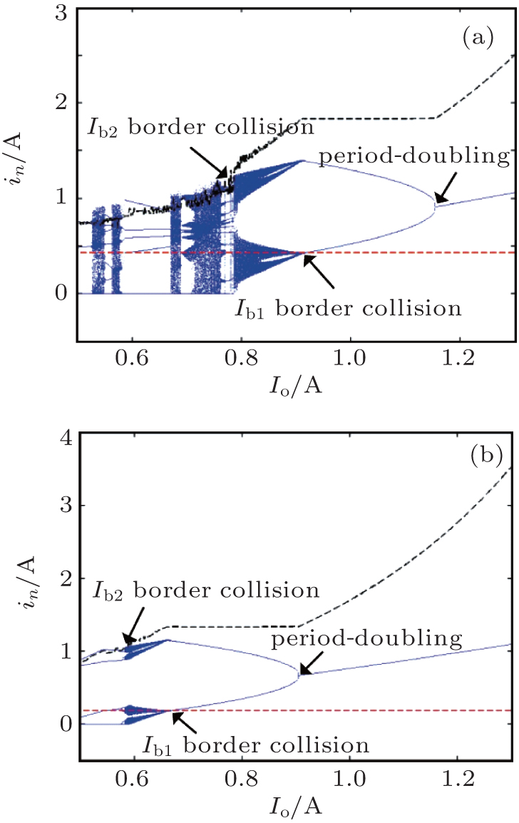 | Fig. 5. Bifurcation diagrams with variation of Io under mc = 1000 (a) and 6000 (b). |
It can be observed from Fig. 5 that the period-doubling bifurcations occur at Io = 1.154 A when mc = 1000 and at Io = 0.904 A when mc = 6000 respectively. The orbit of the converter has a transition from robust chaos in CCM to weak chaos in DCM, which emerges at Io = 0.785 A when mc = 1000, as shown in Fig. 5(a), while the converter enters into the DCM periodic state at Io = 0.583 A from DCM weak chaos occurring at Io = 0.59 A when mc = 6000 as shown in Fig. 5(b). Comparing Fig. 3 with Fig. 5, it is apparent to find that the points of period-doubling bifurcation and border collision bifurcation move leftwards with adopting the ramp compensation, which extends the stable operation region of the converter. Moreover, the area of DCM weak chaos becomes narrower with increasing the slope of the compensation ramp.
Keeping E = 9.7 V, Io = 0.8 A and mc = 0, we can obtain its bifurcation diagram and the corresponding Lyapunov exponent when the proportional coefficient k varies from 0 to 0.4 as shown in Fig. 6. The fastscale accompanied by slow-scale oscillation occurs in a narrow range from 0 to about 0.03. With further increasing the value of k, the converter exhibits fast-scale subharmonic oscillation and enters into CCM chaos at k = 0.07. At the same time, the Lyapunov exponent just turns into a positive value.
 | Fig. 6. (a) Bifurcation diagram and (b) Lyapunov exponent spectrum varying with k. |
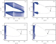
Taking E as the bifurcation parameter with using the same circuit parameters as those in Fig. 6, the inductor current bifurcation diagram can be described in Fig. 7 under different values of k for the further study of its influence on the stability of the converter. To make it more specific, the proportional coefficient in the voltage feedback loop can be set to be 0, 0.02, 0.03 and 0.06 respectively.
 | Fig. 7. Bifurcation diagrams varying with E under k = 0 (a), 0.02 (b), 0.03 (c), and 0.06 (d). |
Comparing Fig. 7 with Fig. 4(a), it is found that the areas of fast-scale and slow-scale subharmonic oscillation exist without the output voltage feedback. The region of slow-scale (low-frequency) oscillation can be gradually removed by increasing k, and then the converter behavior is described with a new bifurcation diagram without slow-scale oscillation (see Fig. 7(d)). Another phenomenon that can be obviously observed from Fig. 7 is that the point of losing stability shifts leftwards slowly, which demonstrates that the stable region can be broadened for a certain range of k.
To verify the analysis results above, different values of k and mc are selected for cycle-by-cycle simulation by Matlab software. Time-domain simulation waveforms and phase portraits of the converter are depicted by the Runge– Kutta algorithm via adopting a piecewise smooth switching model.
When E = 14 V and other parameters are the same as those in Fig. 7, let k = 0, k = 0.02 and k = 0.06 respectively, the inductor current iL values and phase portraits (in the iL– vo plane) of the peak current-mode controlled buck converter with CCL are shown in Fig. 8.
 | Fig. 8. Time-domain waveforms of inductor current and phase portrait in iL– vo plane at k = 0 (a), 0.02 (b), and 0.06 (c). |
Comparing Fig. 8(a) with Fig. 8(b), it can be seen that fast-scale and low-scale oscillation phenomenon are transferred to subharmonic oscillation by using relatively small proportional coefficient k. It can be seen clearly that the converter is stable with k = 0.06 while subharmonic oscillation exists with k = 0.02, which are consistent with the bifurcation diagram in Fig. 7.
Fixing E = 12 V and k = 0, the time-domain waveforms of inductor current iL can be obtained as shown in Figs. 9(a)– 9(c) with different slopes of compensation ramp, i.e., mc = 1000, mc = 2000, and mc = 6000, while figures 9(d)– 9(f) show the waveforms when k = 0.2 at the mc values of 1000, 2000, and 6000, respectively.
 | Fig. 9. Time-domain waveforms of inductor current with (a) k = 0 and mc = 1000; (b) k = 0, and mc = 2000; (c) k = 0 and mc = 6000; (d) k = 0.2 and mc = 1000; (e) k = 0.2 and mc = 2000; (f) k = 0.2 and mc = 6000. |
A comparison among Figs. 9(a)– 9(c) shows that the adoption of ramp compensation can eliminate both fast-scale accompanied by slow-scale oscillation and subharmonic oscillation. Moreover, the bigger the mc, the better the results are. Comparing Fig. 9(a) with Fig. 9(d), it is shown that under the same mc, the converter with a proper output voltage feedback seems to have a better performance due to its influence on slow-scale oscillation. The same conclusion is also inferred by comparing Fig. 9(b) with Fig. 9(e).
The experimental set-up is built with the same circuit parameters as those in the simulation analysis for verifying the simulation results of the stabilization in the peak current-mode controlled buck converter with CCL, by adding the ramp compensation and the output voltage feedback. The experimental results are shown in Fig. 10, in which Figs. 10(a), 10(c), and 10(e) show the waveforms of inductor current when k = 0 with different slopes of compensation ramp, i.e., mc = 1000, 2000, and 6000, while Figs. 10(b), 10(d), and 10(f) display the waveforms when k = 0.2 at mc = 1000, 2000, and 6000 respectively. It is concluded that the fast-scale oscillation accompanied by slow-scale oscillation and subharmonic oscillation can be eliminated gradually with increasing the value of mc, while the adoption of a proper output voltage feedback can wipe off the slow-scale oscillation as indicated by the waveforms in Fig. 10, which agree well with the simulation results shown in Fig. 9, verifying the correctness of the theoretical analysis.
 | Fig. 10. Experimental waveforms of inductor current under (a) k = 0 and mc = 1000; (b) k = 0.2 and mc = 1000; (c) k = 0 and mc = 2000; (d) k = 0.2 and mc = 2000; (e) k = 0 and mc = 6000; (f) k = 0.2 and mc = 6000. |
Assuming xn = [in, vn] and xn+ 1 = [in+ 1, vn+ 1] to be the sampling values of state valuables at nT and (n + 1)T respectively, the fixed point XQ = [I V]T can be solved by making xn+ 1 = xn = XQ while the Jacobi matrix around the XQ can be deduced under the discrete iterative model and shown as follows:

where J11 = ∂ in+ 1/∂ in, J12 = ∂ in+ 1/∂ vn, J21 = ∂ vn+ 1/∂ in, and J22 = ∂ vn+ 1/∂ vn.
If in ≤ Ib1, the elements of the Jacobi matrix are expressed as follows: J11 = cos ω T, J12 = − sinω T/Lω , J21 = ω Lsinω T, and J22 = cosω T.
If Ib1 ≤ in ≤ Ib2, the elements of the Jacobi matrix are expressed as follows:
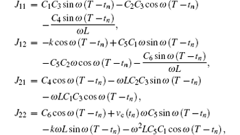
where
and

If Ib2 ≤ in, the elements of the Jacobi matrix are expressed as follows:

where

and

The eigenvalues can be obtained by solving the following characteristic equation:

According to the bifurcation diagrams in Figs. 3 and 4, the case where in ≤ Ib1 will not happen in the area of the period-1 state and its stabilities will be influenced when Ib1 ≤ in ≤ Ib2 in the peak current-mode controlled buck converter with CCL. The period-doubling bifurcation will take place when the eigenvalue equals − 1 and the characteristic equation can be expressed as

Based on Eq. (18), the equation of the stability boundary containing mc and k can be further obtained.
The orbit of the peak current-mode controlled buck converter with CCL is transferred from subharmonic oscillation (period-2 state) to CCM robust chaos when the inductor current reaches the border current Ib1 at the moment when the inductor current is a minimum value. While the inductor current is a maximum value, it reaches the border current Ib2, causing the operation of the converter to shift from CCM to DCM. The two formulas can be obtained as follows:


where

and in+ 1, max = iref
To make it more clearly, two formulas can be deduced further from Eqs. (7)– (9), which give an expression for the two boundary curves. One is the boundary of period-2 state and CCM robust chaos and is expressed as

the other is the boundary of mode transferring from CCM to DCM, and given by

The two formulas both contain mc and k, based on which the boundary curves can be described in parameter maps.
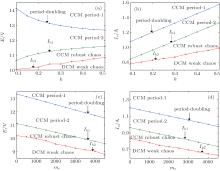
For the engineering applications, it is imperative to illustrate the boundaries of these dynamical behaviors mentioned previously, by knowing all of the operation regions of employing ramp compensation or the output voltage feedback. By exploring the relationships between k and E, k and Io, mc and E, mc and Io, the operation regions can be obtained in the parameter space with the variations of k and mc respectively, owing to the formulas expressed in Eqs. (18), (21), and (22).
As it can be seen from Fig. 11, there are four ways to stabilize the converter: they are to increase E, Io, and mc, and to choose an appropriate value of k. Three operating boundaries including period-doubling, Ib1, and Ib2 divide the work place into CCM period-1 region, CCM period-2 region, CCM robust chaos region and DCM weak chaos region in terms of selected circuit parameters, which provide design-oriented information for ensuring the stable operation of peak current-mode controlled buck converters with CCL.
 | Fig. 11. Operation regions varying with k [(a) k– E and (b) k– Io] and with mc [(c) mc– E and (d) mc– Io]. |
In this paper, we investigate the dynamical behaviors and stabilizations of peak current-mode controlled buck converters with CCL. Discrete iterative map models with two inductor current borders are established to study the complex dynamics of the converter by depicting its bifurcation diagram and Lyapunov exponent spectrum. The influences of the slope mc of the compensation ramp and proportional coefficient k of the output voltage feedback loop on the stability of the converter are explored based on the iterative map model. To testify the validities of simulation and theoretical analysis, the experiment is carried out. The operation regions within variation of k and mc are obtained by analyzing the loss of stabilities and border collision.
Research results in this paper point out that there exist four operation regions in the peak current-mode controlled buck converter with CCL, i.e., CCM period-1, CCM period-2, CCM robust chaos, and DCM weak chaos, which are divided by the period-doubling bifurcation and two boundaries of border collision for the changing of k and mc. It is also concluded that the ramp compensation can eliminate both fast-scale oscillation accompanied by slow-scale oscillation and subharmonic oscillation, broaden the stable area of the converter, and transfer the operation mode. When the output voltage feedback loop is introduced, the fast-scale and slow-scale subharmonic oscillation can be gradually eliminated and the stable region can be extended slowly.
| 1 |
|
| 2 |
|
| 3 |
|
| 4 |
|
| 5 |
|
| 6 |
|
| 7 |
|
| 8 |
|
| 9 |
|
| 10 |
|
| 11 |
|
| 12 |
|
| 13 |
|
| 14 |
|
| 15 |
|
| 16 |
|
| 17 |
|
| 18 |
|
| 19 |
|
| 20 |
|
| 21 |
|
| 22 |
|
| 23 |
|
| 24 |
|
| 25 |
|