Electronic synapses based on ultrathin quasi-two-dimensional gallium oxide memristor
Wang Shuopei1, 2, He Congli1, 3, †, Tang Jian1, 2, Yang Rong1, 4, Shi Dongxia1, 2, 4, Zhang Guangyu1, 2, 4, 5, ‡
CAS Key Laboratory of Nanoscale Physics and Devices; Beijing National Laboratory for Condensed Matter Physics and Institute of Physics, Chinese Academy of Sciences, Beijing 100190, China
School of Physical Sciences, University of Chinese Academy of Sciences, Beijing 100190, China
Institute of Advanced Materials, Beijing Normal University, Beijing 100875, China
Beijing Key Laboratory for Nanomaterials and Nanodevices, Beijing 100190, China
Songshan Lake Materials Laboratory, Dongguan 523808, China


† Corresponding author. E-mail: conglihe@bnu.edu.cn gyzhang@iphy.ac.cn

Abstract

Synapse emulation is very important for realizing neuromorphic computing, which could overcome the energy and throughput limitations of todayʼs computing architectures. Memristors have been extensively studied for using in nonvolatile memory storage and neuromorphic computing. In this paper, we report the fabrication of vertical sandwiched memristor device using ultrathin quasi-two-dimensional gallium oxide produced by squeegee method. The as-fabricated two-terminal memristor device exhibited the essential functions of biological synapses, such as depression and potentiation of synaptic weight, transition from short time memory to long time memory, spike-timing-dependent plasticity, and spike-rate-dependent plasticity. The synaptic weight of the memristor could be tuned by the applied voltage pulse, number, width, and frequency. We believe that the injection of the top Ag cations should play a significant role for the memristor phenomenon. The ultrathin of medium layer represents an advance to integration in vertical direction for future applications and our results provide an alternative way to fabricate synaptic devices.

1. Introduction

Artificial neural networks have shown superior performance over classical systems in processing cognitive and big data tasks. Meanwhile, recent advances in algorithm developments have led to performance even surpassing that of humans in specific complex tasks.[13] Until now, implementations of neural networks have been mainly based on conventional computing hardware, where the memory and processor are physically separated. The data are stored in the memory and need to be constantly loaded into the processing unit to compute the desired output. Consequently, the performance requires enormous computing hardware resources and high power consumption during operation, which is limited by the von Neumann bottleneck.[4,5]

The memristor is a two-terminal electronic device, whose conductance can be precisely modulated by the charge or flux through it. Memristors have been studied extensively for using in non-volatile resistive random-access memory (RRAM).[6] Similar to a biological synapse, memristor can simultaneously store the synaptic weight and modulate the transmitted signal in one single device, which will be very useful for developing neuromorphic computing.[710] As a binary metal oxide, gallium oxide is considered as one of the ideal candidates for RRAM and has been investigated broadly, in which both bipolar and unipolar resistance switching behaviors were observed, indicating the rich and adjustable physical properties of the gallium oxide film.[1115] However, the emulating synaptic behaviors in gallium oxide thin film based memristor have not been reported so far. The gallium oxide was usually deposited by pulsed laser deposition technology or sputtering system, the thickness of which is from several tens to hundreds nm. Recent studies have revealed that the performance of MIM-based memristors might be enhanced by introducing layered two-dimensional (2D) materials into their structure.[1620] Herein, we report the fabrication of ultrathin quasi-2D gallium oxide film by squeegee method, which was made into simple vertical sandwiched devices by conventional micro-nano fabrication. We have been able to emulate synaptic behavior in the vertical memristor with the thinnest medium layer. The ultrathin of the medium layer represents an advance to integration in vertical direction for future applications. Our results provide an alternative way to fabricate synaptic devices with a high integration level when stacked three dimensionally.

2. Experimental procedure
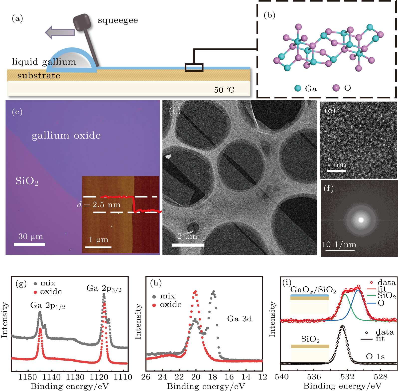
Figure 1(a) demonstrates the squeegee method process. Liquid gallium is placed on a substrate and scraped away to the other side at the hot plate due to low melting temperature of gallium (29.7 °C). When liquid gallium is exposed to ambient atmospheric condition, a smooth thin gallium oxide layer is formed on its surface.[2123] During the squeegee method process, rapid re-oxidation of the metal surface allows continuous deposition gallium oxide film, which resembles a screen-printing process.[2426] To transfer the thin film on arbitrary substrate, the thin gallium oxide layer was made on propylene carbonate (PC) film firstly using squeegee method. Subsequently, the PC film carrying gallium oxide can be attached onto any other targeting substrates such as graphene/SiO2 or TEM grid. Finally, the whole substrate was immersed into acetone to remove PC. The optical image of gallium oxide on a SiO2/Si wafer is shown in Fig. 1(c). Atomic force microscopy (AFM) and transmission electron microscopy (TEM) were used to characterize the samples deposited on top of SiO2/Si wafer and transferred onto TEM grids, respectively. The sample produced by squeegee method featured a smooth surface, seen in the AFM image. The thickness of the thin film is around 2.5 nm, consisting to the previous literature.[25] The structural features and crystal structures of the film were further revealed by TEM (Figs. 1(d)1(f)). The gallium oxide shows amorphous structure, characterized by high-resolution TEM (HRTEM) and selected area electron diffraction (SAED). X-ray photoelectron spectroscopy (XPS) was employed to obtain the chemical bonding states of the thin films. Figures 1(g)1(i) show the spectra of Ga 2p, Ga 3d, and O 1s regions, respectively. The peaks of Ga 2p1/2, 2p3/2, and 3d were observed in gallium oxide samples, while additional peak at lower binding energy corresponding to the metallic state of gallium was observed in gallium oxide/gallium mix samples.[27] Figure 1(i) shows O 1s fitted XPS spectra of SiO2 and GaOx/SiO2. Two different oxide peaks for O 1s were observed when GaOx was deposited on the SiO2. These peaks correspond to SiO2 (binding energy = 532.6 eV) and GaOx (binding energy = 530.8 eV). This indicates that the thin film made by squeegee method is composed of the oxide of the gallium.

Fig. 1. (a) Schematic illustration of formation of a thin gallium oxide layer on liquid gallium surface under atmospheric condition. (b) The structure of gallium oxide. (c) Optical microscope image of gallium oxide on a SiO2/Si wafer. Inset: AFM image of gallium oxide on SiO2. (d)–(f) TEM characterization, with HRTEM images and SAED. (g), (h) XPS spectra of the gallium oxide and gallium/gallium oxide mix. (i) XPS spectra of SiO2 substrate with and without GaOx.
3. Experimental results and discussion

Figure 2(a) schematically shows the two-terminal device structure. The gallium oxide made by squeegee method was transferred onto a few-layer graphene flake which serves as a thin bottom electrode (BE) of the memristor device. Figure 2(b) demonstrates the AFM image of the gallium oxide on few-layer graphene, showing that the surface of the gallium oxide is smooth and clean after transfer. The height profile reveals that the thickness of the gallium oxide is 2.5 nm. Silver was subsequently deposited as the top electrode (TE). The vertical sandwiched structure memristor device was completely fabricated.

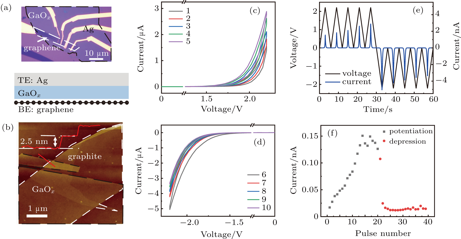
Fig. 2. (a) The optical image of the device (top) and the schematic of the memristor device (bottom). (b) AFM image of GaOx stacked on few layer graphene. (c), (d) Measured IV characteristics of the memristor. (e) The current and voltage data plotted against time for the device in (c) and (d), indicating the variation trend in current in sequential voltage sweeps. (f) The current was obtained after a series of 20 set pulses (2 V, 100 ms, black dots) followed by 20 reset pulses (−2 V, 100 ms, red dots), showing the respective potentiation and depression of the synaptic weight. The reading voltage is 1 V.

The current–voltage (IdVd) characteristics of the heterostructure are shown in Figs. 2(c) and 2(d). Initially, the current of the vertical sandwiched structure increases gradually with the number of sweep when five consecutive positive voltage sweeps are applied to the device. Afterwards, the current decreases continuously when the voltage sweeps is reversed to negative. In order to clearly illustrate the changing trend, the curve of sweeping voltage and the corresponding current versus time are plotted in Fig. 2(e). The current shows continuously increase (decrease) in sequential positive (negative) voltage sweeps obviously. To verify the potential switching mechanism, we performed several additional experiments using different metal electrodes including Au, in which the increase (decrease) trend was not observed. We believe that the movement of the top Ag cations should play a significant role for the memristor phenomenon. Under positive voltage, the Ag cations are injected into the gallium oxide. The localized conducting Ag filaments between the Ag and graphene electrodes are formed which increase the conductance of the device. With additional positive voltage sweeping, more Ag filaments are formed, which induces progressively increasing conductance. Under negative voltage, the Ag cations move back to the Ag electrode, leading to rupture of Ag filaments and decrease of the conductance of the device. Therefore, we infer that the formation and rupture of Ag filaments under the applied voltage should be response for the reliable “analog” switching behaviors. Furthermore, we replaced gallium oxide with mechanically exfoliated multilayer h-BN. The h-BN based sandwiched structure did not show any memristive behavior. The perfect lattice structure of h-BN restraint the Ag cations movement under bias voltage. The h-BN shows permanent breakdown in high electrical field, which is ascribe to defect-free of the h-BN layer.[28,29] Oppositely, the amorphous structure of gallium oxide prepared by squeegee method containing a large amount of defects could be helpful for the memristive behaviors. The advanced study such as in situ TEM analysis of structure should be further performed to understand the exact switching mechanism.[30]

The conductivity of the devices could also be gradually tuned by applying a series of pulses. A continuous 20 positive pulses (2 V, 100 ms) and 20 negative pulses (−2 V, 100 ms) were applied to the device. Figure 2(f) shows the current readout at 1 V bias after each pulse. The read voltage was selected at 1 V (which is not large enough to change the resistance state of the device) because of large on–off ratio around this voltage. The current shows increasing and decreasing gradually along with the positive and negative pulses, which is analogous to the respective potentiation and depression of the synaptic behavior induced by the stimulation sequence.

Figure 3(a) shows a schematic illustration of a biological synapse, which connects a presynaptic neuron and a postsynaptic neuron. A signal is transmitted between neurons by sending neurotransmitters. When an action potential arrives at the presynaptic neuron, the neurotransmitters are released from the presynaptic neuron and go through the synapse to dock with receptors on the postsynaptic neuron, triggering a subsequent action potential in the post-neuron. Then the signal is sent to the next neuro.[31,32] Under external stimuli, spikes or action potentials from presynaptic neurons can be transmitted to the postsynaptic neurons via synapses and produce excitatory postsynaptic currents (EPSC). The synaptic weight represented by the degree of connectivity between the pre- and post-neurons is simply described by EPSC. Similar to this architecture, in our vertical sandwiched memristor, the top and bottom electrodes work as the pre- and post-synaptic neurons, respectively. The two-terminal memristor could be used to mimic the synaptic behaviors in neurons. The conductance of the device, considered as synaptic weight, can be modulated by pulse voltage applied to either electrodes. The increase or decrease of conductivity represents potentiation or depression of the synaptic weight in response to the potentiating and depressing spikes.

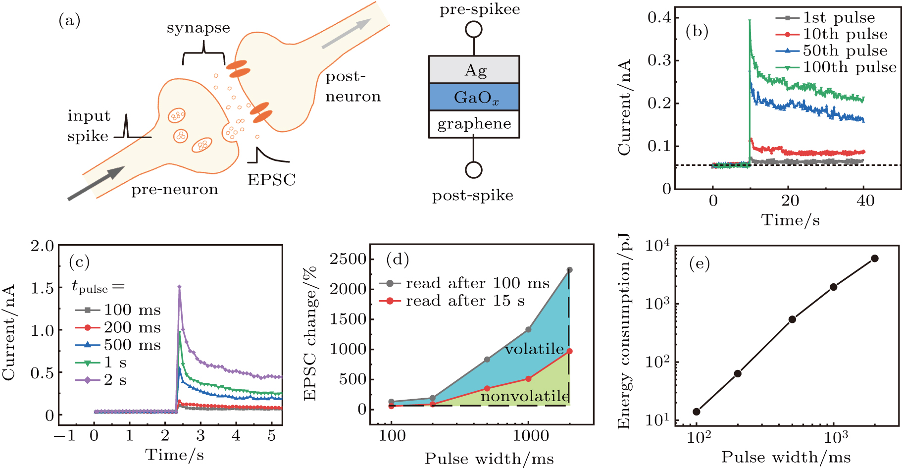
Fig. 3. (a) Illustration of a biological synaptic junction between the presynaptic and postsynaptic neurons (left) and the schematics of the two-terminal device geometry structure (right). (b) The EPSC decay after applying the 1st, 10th, 50th, and 100th pulses (100 ms, 2 V, separated by 1000 ms). (c) EPSC is triggered by one pulse with different pulse width time. The pulse amplitude was fixed at 2 V. (d) EPSC change ratio (II0)/I0 ×100% by reading after 100 ms and 15 s for different pulse width time. (e) The energy consumption during a single pulse with different pulse width time.

Figure 3(b) shows the EPSC obtained by applying the 1st, 10th, 50th, and 100th pulse voltages (100 ms, 2 V). The EPSC shows a sudden increase simultaneous with applying the presynaptic pulse and decays back gradually to the steady current. The relaxation time constant (τ) of the EPSC increases from 0.61 s to 23.77 s with increasing pulse number, indicating a trend of transition from short time memory (STM) to long time memory (LTM) behavior.[10,33] This happens because more silver cations are injected into the middle medium layer with increasing pulse number.

The EPSCs induced by presynaptic pulses with different pulse width time are shown in Fig. 3(c). The amplitudes of the EPSC increase with increasing pulse width time from 100 ms to 2 s. Figure 3(d) shows the EPSC change ratio under different read time. The steady EPSC after 15 s is enhanced significantly with increasing pulse width time, indicating a trend of transition from STM to LTM, which is similar to the observed phenomenon as increasing pulse number. The memristor shows a current of ∼50 pA at a read voltage of 1 V after the voltage pulse with the amplitude of 2 V and duration time of 100 ms. The power consumption (Pstandby=Iread×Vread) in standby is 50 pW. Figure 3(e) shows the energy consumption under different pulse width extracted from Fig. 3(c). The energy consumption for one pulse is calculated by W=Ipeak ×Vpulse ×t, where Ipeak, Vpulse, and t represent the peak value of the EPSC, the pulse voltage, and the pulse width, respectively. The energy consumption decreases rapidly with the decrease of the pulse width. The smallest energy consumption is about 14 pJ (100 ms), which is two orders of magnitude lower than that of an artificial synapse based on conventional CMOS circuits ( per stimulation).[4] It is reasonable to estimate that the energy consumption of our devices can be further reduced by decreasing the pulse width time.

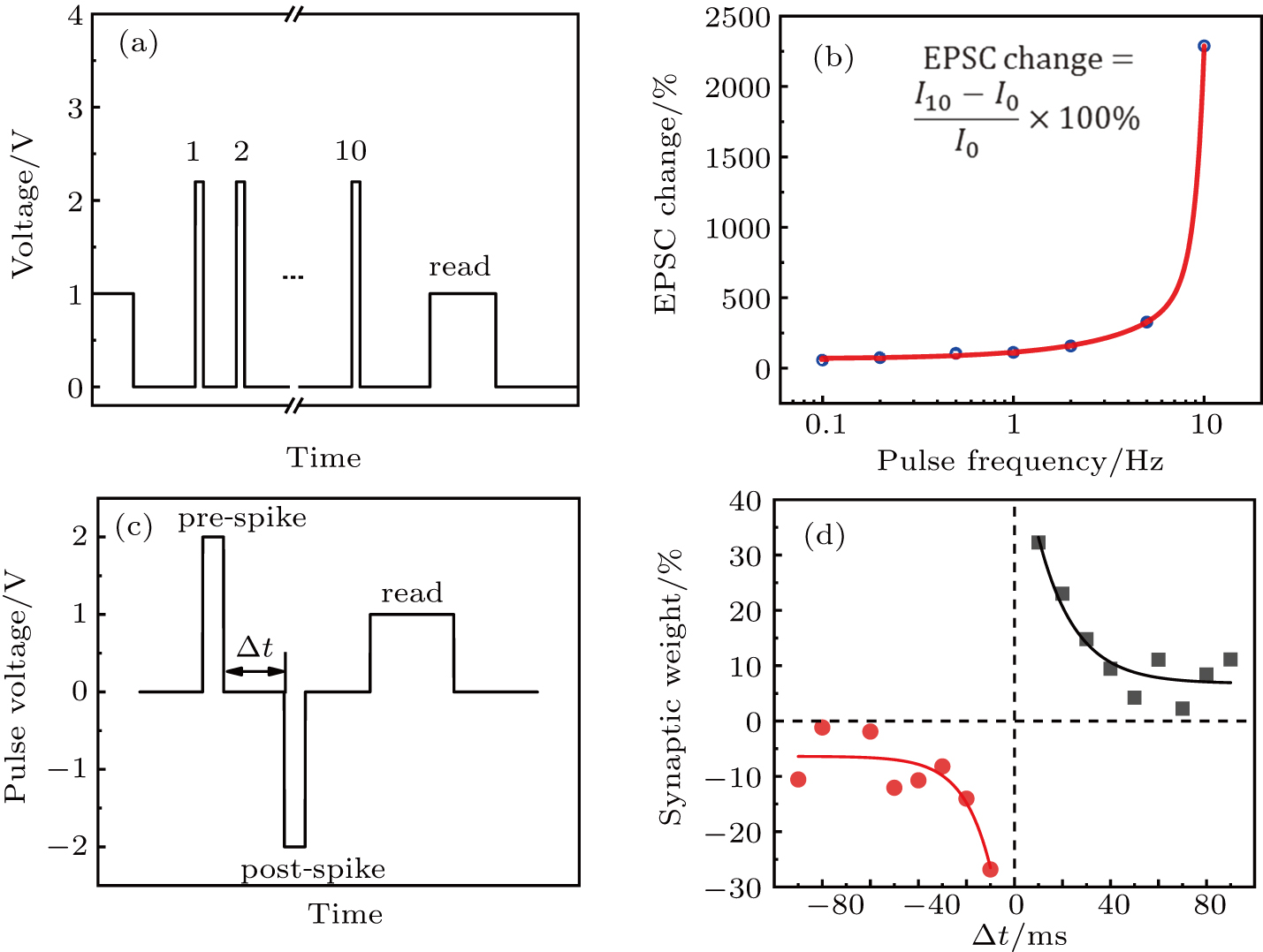
Besides the pulse width time and pulse number, the applied pulse frequency can also affect the synaptic weight. This is similar to the biological phenomenon referred to as spike-rate-dependent plasticity (SRDP). To demonstrate SRDP, 10 identical value pulses with different frequencies from 0.1 Hz to 10 Hz were applied to the memristor, as shown in Fig. 4(a). The pulse amplitude was fixed at 2 V and the pulse widths were 100 ms. The EPSC change was detected by calculating the change ratio I10/I0, where I10 is the current after 10 pulses and I0 is the initial current under the reading voltage of 1 V. The EPSC change drastically increases at higher pulse frequency (Fig. 4(b)), indicating that the synaptic weight could also be changed through changing the applied pulse frequency.

Fig. 4. (a) The schematic illustration of SRDP. 10 consecutive pulses were applied then read the EPSC. The pulse amplitude and reading voltage were fixed at 2 V and 1 V, respectively. The pulse widths were 100 ms. (b) EPSC changes as a function of frequency. (c) Experimental setup of STDP, a positive and negative pulse pair was applied on the pre-synaptic side. The positive pulse equals to pre-synaptic spike and negative pulse equals to post-synaptic spike. (d) Change of the synaptic weight as a function of the relative timing between the pre- and post-synaptic pulses, .

Spike-timing-dependent plasticity (STDP), as a basis for the Hebbian learning rule, is a biological process that adjusts the strength of connections between neurons in the brain.[31] To demonstrate the STDP learning rule, we applied a pulse pair to the TE while ground the BE. The pulse pair we used contains a positive pulse representing the presynaptic spike and a negative pulse representing the postsynaptic spike, as shown in Fig. 4(c). This is equivalent to applying identical positive pulses to both pre- and post-synaptic sides of the memristor. The two pulses were separated by a time difference , where tpre (tpost) represent the time when the presynaptic neuron (postsynaptic neuron) spikes. Figure 4(d) shows the measured change of the synaptic weight versus Δ t. When the pre-synaptic spike arrives ahead (behind) the post-synaptic spike, the synaptic weight of the memristor increases (decreases). This observation can be attributed to the intrinsic decay trend of the EPSC in our device, which enables us to realize the STDP function by the simple pulse pair instead of complicated designed external preprogramming.[8,34] Moreover, the change in the synaptic weight versus the spike timing difference Δ t can be well fitted with exponential decay functions, indicating that STDP characteristics are similar to those of biological synapse.[35,36]

4. Conclusion

In summary, we have demonstrated an ultrathin synaptic memristor based on quasi-2D gallium oxide for the first time. The ultrathin and smooth gallium oxide layer was prepared by the squeegee method, which is suitable for other low melting temperature metals or eutectic alloys such as Sn and galinstan. The essential functions of biological synapses, including depression and potentiation of synaptic weight, transition from STM to LTM, SRDP, and STDP, have been demonstrated in the two-terminal memristor. These findings provide an alternative way to fabricate synaptic devices based on atomically thin metal oxides and the ultrathin of medium layer represents an advance to integration in vertical direction for future applications.

Reference
[1] Yegnanarayana B 2009 Artificial Neural Networks PHI Learning Pvt. Ltd.
[2] Silver D Schrittwieser J Simonyan K Antonoglou I Huang A Guez A Hubert T Baker L Lai M Bolton A 2017 Nature 550 354
[3] Ananthanarayanan R Esser S K Simon H D Modha D S 2009 Proceedings of the Conference on High Performance Computing Networking, Storage and Analysis p. 63
[4] Indiveri G Chicca E Douglas R 2006 IEEE Trans. Neural Netw. 17 211
[5] Izhikevich E M Edelman G M 2008 Proc. Natl. Academy Sci. 105 3593
[6] Chua L 1971 IEEE Trans. Circuit Theory 18 507
[7] Lee M J Lee C B Lee D Lee S R Chang M Hur J H Kim Y B Kim C J Seo D H Seo S 2011 Nat. Mater. 10 625
[8] Jo S H Chang T Ebong I Bhadviya B B Mazumder P Lu W 2010 Nano Lett. 10 1297
[9] Strukov D B Snider G S Stewart D R Williams R S 2008 Nature 453 80
[10] Ohno T Hasegawa T Tsuruoka T Terabe K Gimzewski J K Aono M 2011 Nat. Mater. 10 591
[11] Guo D Y Wu Z P An Y H Li P G Wang P C Chu X L Guo X C Zhi Y S Lei M Li L H Tang W H 2015 Appl. Phys. Lett. 106 042105
[12] Guo D Y Wu Z P Zhang L J Yang T Hu Q R Lei M Li P G Li L H Tang W H 2015 Appl. Phys. Lett. 107 032104
[13] Aoki Y Wiemann C Feyer V Kim H S Schneider C M Ill-Yoo H Martin M 2014 Nat. Commun. 5 3473
[14] Hsu C W Chou L J 2012 Nano Lett. 12 4247
[15] Gao X Xia Y Ji J Xu H Su Y Li H Yang C Guo H Yin J Liu Z 2010 Appl. Phys. Lett. 97 193501
[16] Wang M Cai S Pan C Wang C Lian X Zhuo Y Xu K Cao T Pan X Wang B Liang S J Yang J J Wang P Miao F 2018 Nat. Electron. 1 130
[17] Zhao H Dong Z Tian H DiMarzi D Han M G Zhang L Yan X Liu F Shen L Han S J Cronin S Wu W Tice J Guo J Wang H 2017 Advanced Mater. 29 1703232
[18] Sangwan V K Lee H S Bergeron H Balla I Beck M E Chen K S Hersam M C 2018 Nature 554 500
[19] Huh W Jang S Lee J Y Lee D Lee D Lee J M Park H G Kim J C Jeong H Y Wang G Lee C H 2018 Adv. Mater. 30 e1801447
[20] Yang C S Shang D S Liu N Shi G Shen X Yu R C Li Y Q Sun Y 2017 Advanced Mater. 29 1700906
[21] Cabrera N Mott N F 1949 Rep. Prog. Phys. 12 163
[22] Regan M J Tostmann H Pershan P S Magnussen O M DiMasi E Ocko B M Deutsch M 1997 Phys. Rev. 55 10786
[23] Zavabeti A Ou J Z Carey B J Syed N Orrell-Trigg R Mayes E L Xu C Kavehei O O’mullane A P Kaner R B 2017 Science 358 332
[24] Lawrenz F Lange P Severin N Rabe J P Helm C A Block S 2015 Langmuir 31 5836
[25] Carey B J Ou J Z Clark R M Berean K J Zavabeti A Chesman A S Russo S P Lau D W Xu Z Q Bao Q Kevehei O Gibson B C Dickey M D Kaner R B Daeneke T Kalantar-Zadeh K 2017 Nat. Commun. 8 14482
[26] Syed N Zavabeti A Ou J Z Mohiuddin M Pillai N Carey B J Zhang B Y Datta R S Jannat A Haque F Messalea K A Xu C Russo S P McConville C F Daeneke T Kalantar-Zadeh K 2018 Nat. Commun. 9 3618
[27] Kim D Thissen P Viner G Lee D W Choi W Chabal Y J Lee J B 2013 ACS Appl. Mater. Interfaces 5 179
[28] Hattori Y Taniguchi T Watanabe K Nagashio K 2015 ACS Nano 9 916
[29] Shi Y Liang X Yuan B Chen V Li H Hui F Yu Z Yuan F Pop E Wong H S P Lanza M 2018 Nat. Electron. 1 458
[30] Yang Y Huang R 2018 Nat. Electron. 1 274
[31] Caporale N Dan Y 2008 Annu. Rev. Neuroscience 31 25
[32] Wang Z Joshi S Savel’ev S E Jiang H Midya R Lin P Hu M Ge N Strachan J P Li Z 2017 Nat. Mater. 16 101
[33] Chang T Jo S H Lu W 2011 ACS Nano 5 7669
[34] Kuzum D Jeyasingh R G Lee B Wong H S P 2012 Nano Lett. 12 2179
[35] Bi G Q Poo M M 1998 J. Neuroscience 18 10464
[36] Song S Miller K D Abbott L F 2000 Nat. Neuroscience 3 919