1. IntroductionAs a form of high electromagnetic wave, high-power microwave (HPM) will cause the semiconductor device to fail or burn out through the front door coupling and the back door coupling,[1] thereby affecting the normal operation of the whole circuit system. With electronic information technology development, the electromagnetic environment is becoming more and more complex. The influence of HPM on modern semiconductor devices and circuit systems has received increasing attention.[2–12]
A simulation of a bipolar junction transistor (BJT) with the high electromagnetic pulses injection from the collector was simulated by utilizing the finite difference time domain method in two dimensions, the results indicated that the damage spot lay between the emitter and the collector where the avalanche breakdown occurs.[13] The transient response characteristics were simulated using the improver two-dimensional semiconductor device simulation program in order to obtain the damage effect of the BJT under the injection of electromagnetic pulse, which showed that the peak temperature appears on the edge of the emitter.[14] In Ref. [15], a typical silicon-based n+–p–p–n+ structure of BJT caused by HPM is built, the simulation results revealed that the most vulnerable point of the device located at the cylinder of the base–emitter junction with the signals injected from the collector. Besides, the device is more easily destroyed with the signals injected from the base compared with the signals injected from the collector. In Ref. [16], the HPM pulse signal is injected into the base of a BJT, both the simulation results and the experimental results demonstrated that the induction voltage pulse generated by the HPM signal resulted in the destruction of the base area and a large amount of fuse and defects, which cause the device to fail. The effect of electromagnetic pulses (EMP) on a BJT with the base injection was investigated by numerical simulation and theoretical study, it was found that the hot spot is located at the edge of the base because the peak value of the electric field and the current density are at this point, where the heat generation is concentrated, and the energy needed for burnout is the smallest compared with two other forms of injection.[17] The amplitude of the injection pulse signal at the base is one of the influencing factors on the damage mechanism and damage points,[18] the simulation results showed that the transistor was destroyed by reverse avalanche breakdown of the base–emitter junction at low pulse amplitude, and the transistor was burned out due to secondary breakdown of the p–n–n+ diode consisting of the base region, epitaxial layer, and substrate at the high pulse amplitude. The damage effect experiment on a silicon low-noise amplifier (LNA) with base terminal injected microwave pulse signal was carried out, indicating that the local silicon material will be eroded and damaged at the base region as long as the microwave power is large enough, which leads to the short-circuit of the base–emitter and the base–collector junction, resulting in the failure of the transistor.[19] Using a combination of the simulation and the experimental results, the energy injected tests on an Si and GaAs bipolar LNA were performed, the results demonstrated that the damage point was between the base and emitter of T2. Meanwhile, the experiments on a silicon LNA showed that the passive resistance inside the LNA is also a vulnerable and weak link under the action of external energy.[20–22]
A composite transistor is widely used in large load driving circuits, power amplifier circuit, switch circuit, and automatic control circuit because of its advantages such as large current, high gain, small volume, fast switching speed, and easy integration. To improve the gain and the stability of the composite transistor, two kinds of structures are proposed, which are hybrid and monolithic composite transistor structures, recently.[23–25] However, researchers focused more on the gain and the stability of composite transistor than its damage effects caused by the harmful electromagnetic wave, so it is of great significance to study the influence of high-power microwave on this device. In this paper, a two-dimensional electro-thermal model of a silicon monolithic composite transistor is established for the first time by using the device simulator, Sentaurus-TCAD. The damage effect and mechanism is studied with the injection of HPM signal into the collector (output port) or base (input port) of the device, and the microwave pulse-width effects are given at the end of this paper. Moreover, we give a comparison of the simulation results and the experimental results, which verifies the correctness of the works.
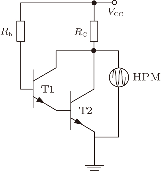
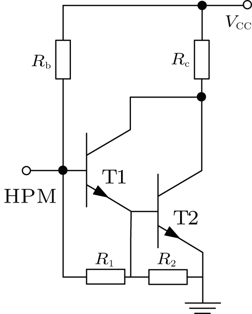
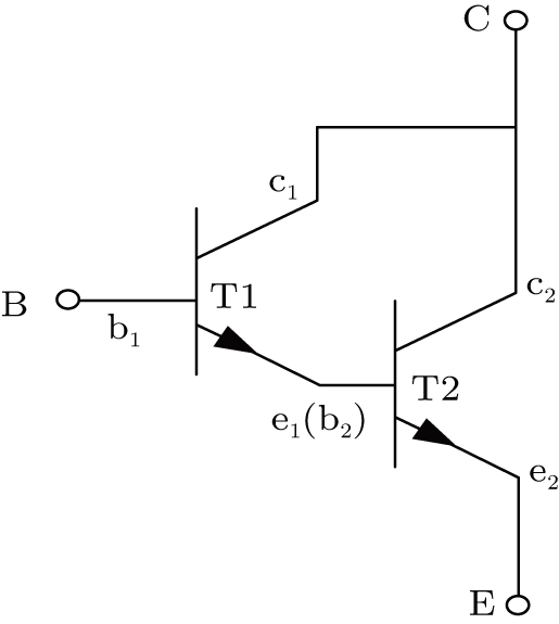
2. Structure and model2.1. Device structureA circuit structure of the composite transistor used in our simulation is illustrated in Fig. 1. In this paper, the composite transistor utilizes two consistent NPN bipolar transistors, that is, T1 and T2 s, in accordance with the same polarity connection and the same power threshold. B, C, and E represents its base, collector, and emitter. The base of T1 (b1) is the base of the composite transistor, the emitter of T2 (e2) is the emitter of the composite transistor, and the common collector of T1 (c1) and T2 (c2) is the collector of the composite transistor. The emitter of T1 (e1) is connected with the base of T2 (b2) through metal. The current is amplified step by step through the T1 and T2 s.
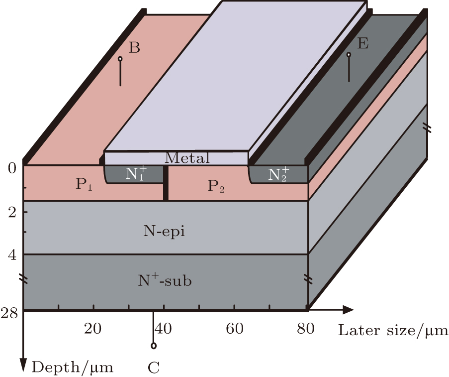
Figure 2 shows a three-dimensional view of the monolithic composite transistor structure.
 is the emitter region of T1 where the doping method is Gauss doping with a surface concentration of 4 × 1019 cm−3, P1 is the base region of T1 where the doping mode is uniform doping with doping concentration of 2 × 1017 cm−3. N-epi is the 2.4-μm-thick n-type epitaxial layer with doping concentration 5 × 1015 cm−3. N+-sub represents the 24-μm-thick collector substrate of the n-type silicon with doping concentration 5 × 1019 cm−3. The thermal electrode is specified at the bottom of the composite transistor, where the lattice temperature maintains at 300 K. The upper surface and the sidewall boundaries are thermally insulated from the environment.
2.2. Numerical modelTo investigate the damage effects and mechanism of the composite amplifier, it is necessary to compute the electrical behavior of the device by employing a device simulator to iteratively solve the Poisson equation and the current-continuity equations. Owing to the high bias voltage and current of the device during microwaves signal injecting, the contribution of the temperature gradient to the current density should be taken into consideration, the current density equation of electrons and holes is modified to
where
μn (
μp) is the electron (hole) mobility,
ϕn (
ϕp) is the electron (hole) quasi-Fermi potential, and
Pn (
Pp) is the electron (hole) absolute thermoelectric power.
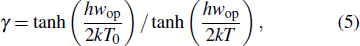
Besides, the effect of the internal temperature of the device on the carrier generation–recombination process needs to be taken into account. The carrier generation–recombination process considers carrier avalanche generation, SRH, and Auger recombination on which it takes the effect of doping concentration and temperature. An avalanche model named the van Overstraeten–de Man model[26] is used to describe the generation process of the electron–hole pair, and avalanche generation rate G is
where
νn(
νp) is the electron (hole) drift velocity,
αn(
αp) is the electron (hole) ionization rate,
α(
E) and
γ are given by
where
hωop is optical phonon energy, ∇
φ is the quasi-Fermi potential, and
a and
b are the default coefficients in the model.
In this paper, the HPM signal model is equivalent to a sinusoidal signal, the mathematical expression is as follows:
where
U0 is the amplitude,
f is the frequency, and
φ is the initial phase. Device failure is indicated when the local lattice temperature reaches the melting point of silicon at 1688 K.
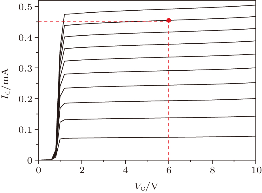
3. Results and discussionThe input–output characteristic curve of the monolithic composite transistor is plotted in Fig. 3, therefore, quiescent dc operation point is set to VCEQ = 6 V, ICQ = 0.45 mA, VBEQ = 1.4 V, IBQ = 0.9 μA, and the values of VCC, Rb, and Rc are set to 9.0 V, 8.4 MΩ, and 6.7 KΩ, respectively.
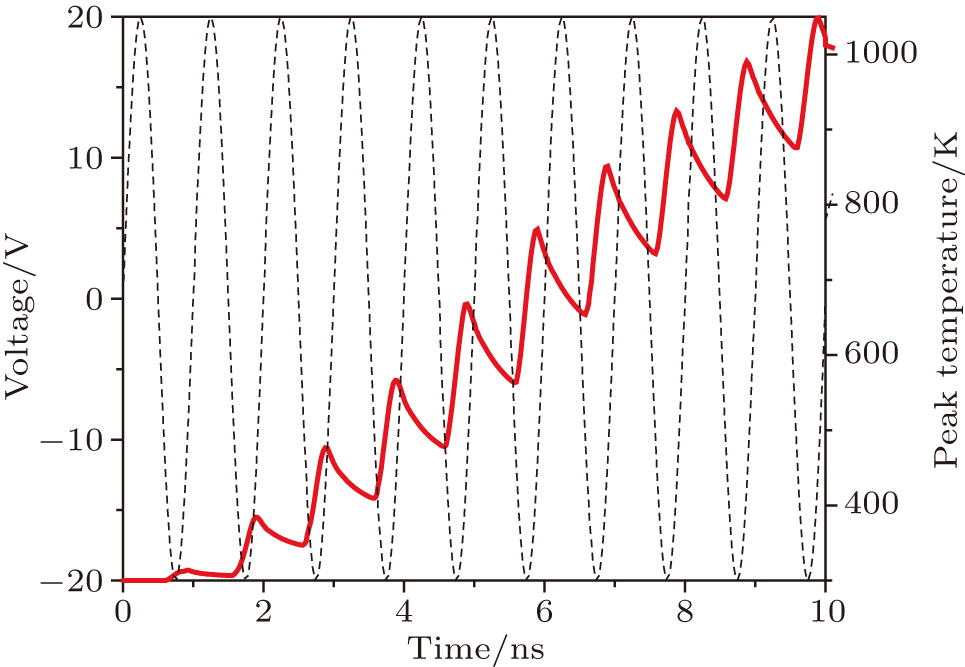
3.1. Damage effect and mechanism under the injection of output portA schematic representation of the composite transistor operating in the state of amplification is shown in Fig. 4. The sinusoidal voltage signal with a frequency of 1 GHz and an amplitude of 20 V is used to study the damage process by injecting directly into the output port of the device. Figure 5 shows the variation of the peak temperature of the device with time from 0 ns to 10 ns. We can see that the variation is characterized by period trends, and the device burns out with continued signal injected. The analysis is based on the fourth cycle in this part. Obviously, the maximum temperature decreases in the positive half-period, while in the negative half-period, there is a trend of increasing firstly and then decreasing. Overall, the peak temperature rises in a cycle.
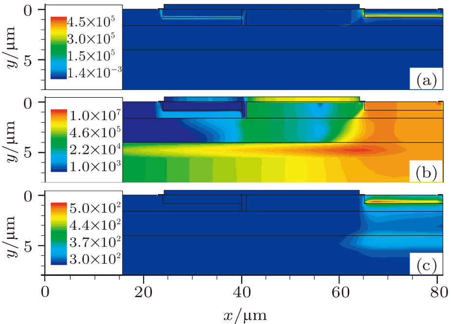
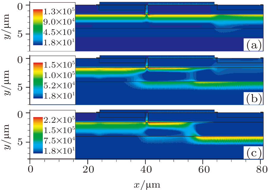
At the beginning of the negative half-period, the composite transistor is in the active mode of operation. When the absolute value of the signal voltage is increased to 1.25 V, the base–emitter junction of T1 and T2 s is reverse-biased while the base–collector junction is forward-biased. It should be noted that the electric field strength (E) of the base–emitter junction of T2 is higher than that of T1 because the voltage drop is mainly across the base–emitter junction of T2, so the peak value of E lies in the edge of the base–emitter junction of T2 (see Fig. 6(a)). The avalanche breakdown would occur near the edge of the base–emitter junction of T2 when E reaches 3.0 × 10⁵ V/cm, which causes the reverse bias current increasing and flowing to the substrate of T2 transistor through the n–n+ layer. From Fig. 6(b), we can see that there are two peak current densities (J) within the device, one is near the edge of the base–emitter junction of T2 and the other is at the n–n+ layer of T2, and the latter is larger than the former. The thermal accumulation produced by power dissipation makes the device temperature increasing, and power density is the expression of E and J. According to the dissipation of E and J in the negative half-period, the main power dissipation point is near the edge of the base–emitter junction of T2, which results in the peak temperature appearing there, too (see Fig. 6(c)). At t = 3.88 ns, the local temperature of the device reaches the highest value up to 566 K. Then the reverse bias voltage across the base–emitter junction of T2 has a decrease with the absolute value of the injected signal voltage decreasing, which causes the peak temperature of the device to begin to decrease at this period.
At the beginning of the positive half-period, the base–emitter junction of T1 and T2 is forward-biased, and the base–collector junction is reverse-biased, which means that the composite transistor is in the active mode of operation. The distribution of E is shown in Fig. 7(a). With the applied signal voltage increasing, the space charge region of the base–collector junction of T2 would extend to the border of the epitaxial layer and the low-resistance n+ substrate since the doping concentration in the base area is higher than that of the collector region (see Fig. 7(b) and Fig. 7(c)).
The peak electric field lies in the n–n+ interface due to the effect of space charge modulation. The avalanche breakdown occurs when E reaches 3.0 × 10⁵ V/cm at the n–n+ layer, the emitter current of T2 flows to the collector substrate through the epitaxial layer, meanwhile, the maximum current density located at the edge of the base–emitter junction of T2 and n–n+ layer (see Fig. 8(a)), particularly, the latter is smaller than the former. The joule heat produced by power consumption lie mainly in the n–n+ layer in the positive half-period, and the thermal accumulation at the base–emitter junction of T2 is reduced at this time. However, the values of the E and J in the positive half-period are about 2.2 × 10⁵ V/cm and 2.6 × 10⁶ A/cm2, respectively, while 4.5 × 10⁵ V/cm and 1 × 10⁷ A/cm2 in the negative half-period, which causes the temperature at the base–emitter junction of T2 to still be higher than the temperature at the n–n+ interface in the positive half-period (see Fig. 8(b)).
A conclusion can be made from the previous analysis that the peak temperature of the composite transistor decreases in the positive half-period, while the temperature elevation of the device occurs in the negative half-period. With the signal voltage continued, the maximum temperature variations have a periodic trend of “decrease–increase” until the temperature at the damage point reaches the melting point of silicon.
3.2. Damage effect and mechanism under the injection of input portIn this section, the damage process is explored when the sinusoidal voltage signal with an amplitude of 15 V is injected directly into the input port of the device. The simulation circuit is plotted in Fig. 9. The following analysis is based on the relationship between the peak temperature and simulation time in the third cycle.
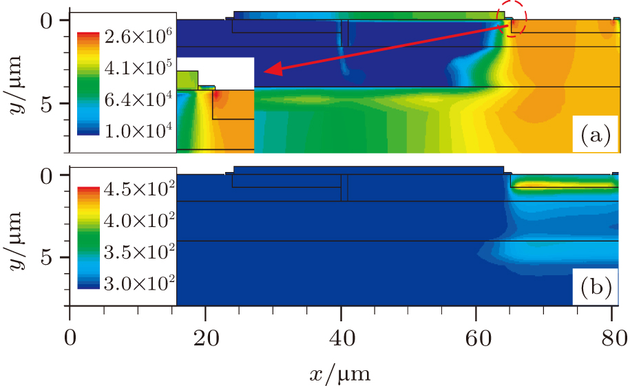
In the positive half-period, with the amplitude of the signal increasing, both the B–E junctions of T1 and T2 are forward-biased, which causes the forward current flowing through these two pn junctions, and the current grows exponentially. Particularly, the current concentrates upon the edge of the pn junction and the magnitude of the current is large (107 A/cm2). The temperature variation within the device is mainly affected by the current density with the input port injection, besides, considering the effect of protection resistances on T1, the current density of the B–E junction of T2 is larger than that of T1 (see Fig. 10(a)), which leads to the peak temperature of the device apearing between the base and emitter of T2. In the negative half-period, both the B–E junction of T1 and T2 are reverse-biased, there exists a large reverse current (106 A/cm2) at the edge of the B–E junction of T1 and T2 when the amplitude of the reverse voltage is large enough (see Fig. 10(b)), therefore, the peak temperature also increases in the negative half-period.
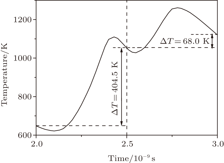
As shown in Fig. 11, the peak temperature increases by 404.5 K in the positive half-period, while only 68.0 K in the negative half-period. This is because the current density in the positive half-period is greater than that in the negative half-period.
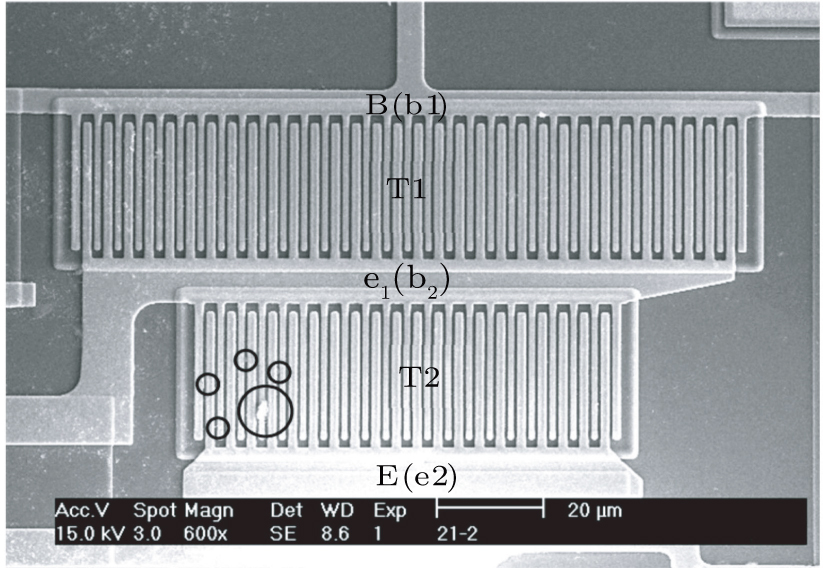
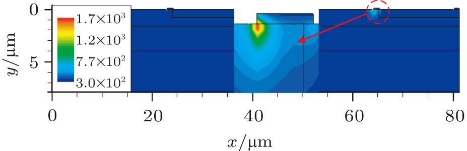
Figure 12 shows the distribution of the temperature inside the device at burning time with the input injection. We can know from the figure that there is only one damage point which is between the base and the emitter of T2. Experiments of the energy injection into the silicon bipolar low-noise amplifiers (LNA) are performed by introducing pulse modulated signal at LNAs inputs.[20] The experiment results show that the damage point is located between the base and emitter of T2 (see Fig. 13). Therefore, we conclude that the simulation results in this paper are in line with experiment results, and the model of the monolithic composite transistor could be used to analyze the damage effects induced by the high-power microwave well.
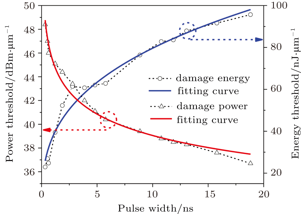
3.3. Pulse-width effects with the HPM injectionTo provide a good prediction of semiconductor device damage and a guiding significance for HPM destruction, the dependence of the damage power threshold, P, and the damage energy threshold, E on the pulse-width under the output and input injection are obtained. In this paper, the pulse-width (τ) is defined as the time duration of the injected signal before the device is burned down, and the damage power threshold and the damage energy threshold as the average power and the total absorbed energy, respectively.
The variations of P and E with τ under the injection of output port are shown in Fig. 14, which demonstrate that the damage power threshold of the device decreases with the increase of pulse-width, while the damage energy threshold increases. The pulse-width versus the damage power threshold and the damage energy threshold obey the following formulas:
the correlation coefficients of Eq. (
7) and Eq. (
8) are 0.98 and 0.97, respectively, which shows a high degree between the pulse-width and the damage power threshold and the damage energy threshold, respectively.
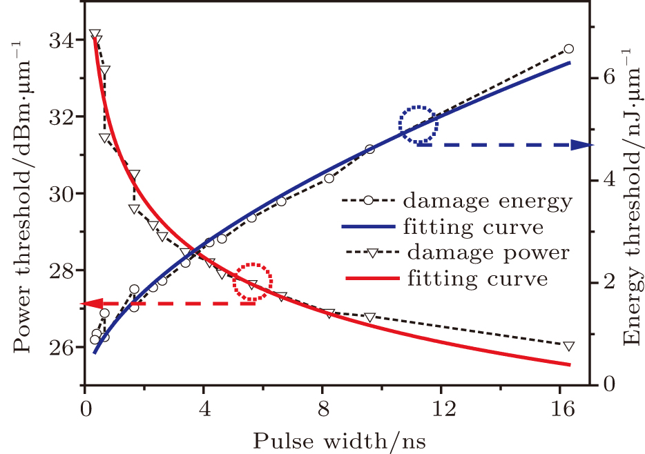
The dependence of the damage power and the damage energy on the pulse-width with the input injection are illustrated in Fig. 15. The following two expressions are obtained by the curve fitting software:
the correlation coefficients of Eq. (
9) and Eq. (
10) are 0.97 and 0.98, respectively. The formulas obtained conform to the empirical formula for short electromagnetic pulse from the experimental results of Wunsch, Bell, and Tasca.
[27,28]Comparing Fig. 14 with Fig. 15, we can make a conclusion that smaller values of the damage power and the damage energy under the input injection are needed to destroy the device than those under the output injection for a mixed pulse-width. In other words, the input injection is more likely to damage the device than the output injection. The conclusion in this paper is consistent with previous work.[15,17] Therefore, the power and energy threshold equations obtained in this paper can predict the damage of the composite transistor very well.
4. ConclusionIn this paper, a two-dimensional model of a silicon NPN monolithic composite transistor structure is established firstly using the semiconductor device simulator. A detailed investigation on the damage process and mechanism caused by HPM is performed by analyzing the distribution of electric field, current density, and temperature of the device. The analysis reveals that temperature elevation processes appear in the negative half-period because both the peak electric field and the maximum current density lie in the edge of the B–E junction of T2 when HPM is injected from the output port, while the temperature decreases in the positive half-period. There is only one hot spot under the output injection, which locates near the edge of the B–E junction of T2, while for the injection from the input port, the damage point exists between the base and the emitter of T2. Compared with the output port injection, the input port injection is easier to destroy the device. By adopting the fitting software, the dependence of the damage energy, E, and the damage power, P, on pulse-width are obtained, respectively. The fitting formulas demonstrate that the damage energy threshold rises while the power threshold falls with the pulse-width increasing. Furthermore, the simulation results in this paper have a good coincidence with the experiment results. The findings of this paper are helpful to investigate the mechanism and protection of high-power microwave damage on semiconductor devices and circuits.


