Image charge effect on the light emission of rutile TiO2(110) induced by a scanning tunneling microscope*
Project supported by the National Key R&D Program of China (Grant Nos. 2016YFA0300901 and 2017YFA0205003), the National Natural Science Foundation of China (Grant Nos. 11634001 and 21725302), and the Key Research Program of the Chinese Academy of Sciences (Grant No. XDPB08-1).
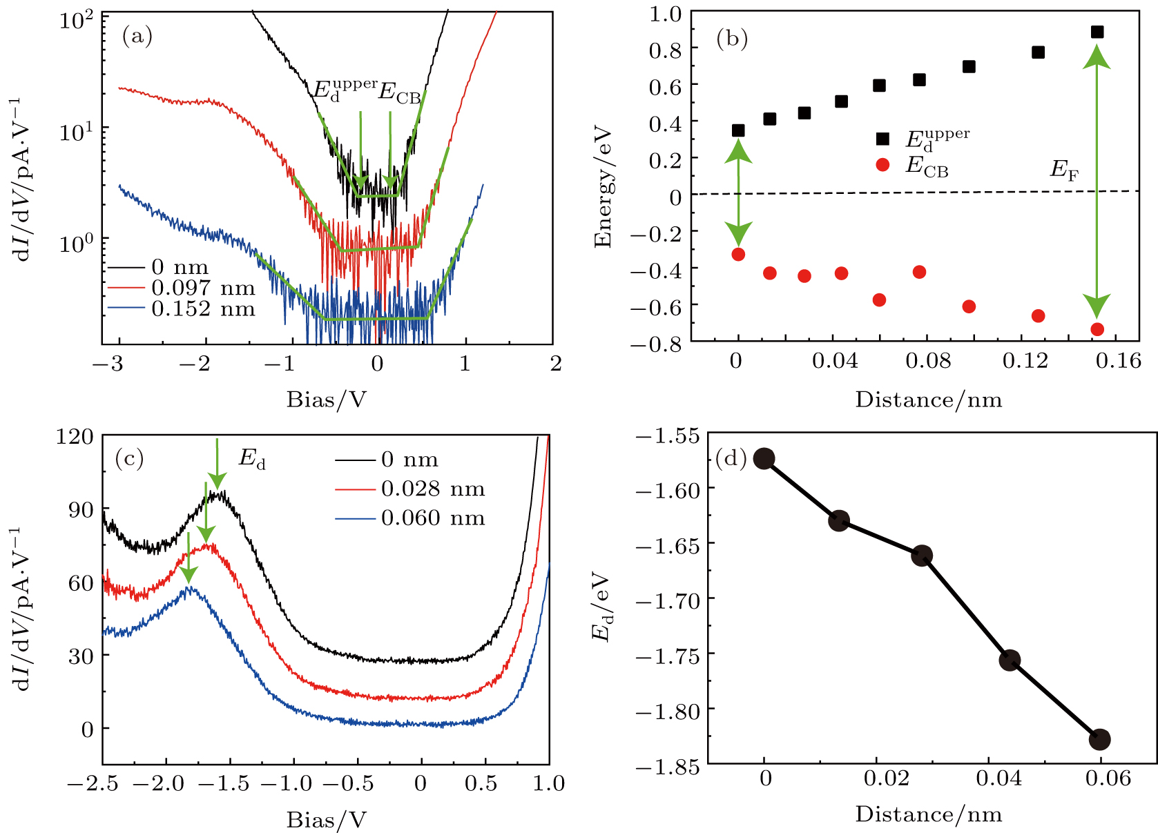
(color online) (a) dI/dV spectra taken at the defective TiO2(110) surface with different tip-sample distance in Logarithmic scale. The tip heights refer to the set point of 1.7 V/0.8 nA (0 nm). The spectrum taken at 0.097 nm and 0 nm were offset by 1.2 pA/V and 3.6 pA/V for clarity, respectively. The band edges are denoted by green arrows. (b) Band edge energies derived from the dI/dV spectra at different tip-sample distances. The green double-headed arrows show the energy gap between the conduction band and defect states. (c) dI/dV spectra taken at the same area in linear scale. The tip heights refer to the set point of 1.7 V/0.8 nA (0 nm). The spectrum taken at 0.028 nm and 0 nm were offset by 12 pA/V and 27 pA/V for clarity, respectively. The green arrows indicate the peak position of defect states (Ed). (d) The energy of defect states (Ed) as a function of tip-sample distance.