Image charge effect on the light emission of rutile TiO2(110) induced by a scanning tunneling microscope*

Project supported by the National Key R&D Program of China (Grant Nos. 2016YFA0300901 and 2017YFA0205003), the National Natural Science Foundation of China (Grant Nos. 11634001 and 21725302), and the Key Research Program of the Chinese Academy of Sciences (Grant No. XDPB08-1).

Guo Chaoyu1, Meng Xiangzhi1, Wang Qin1, Jiang Ying1, 2, 3, †
       

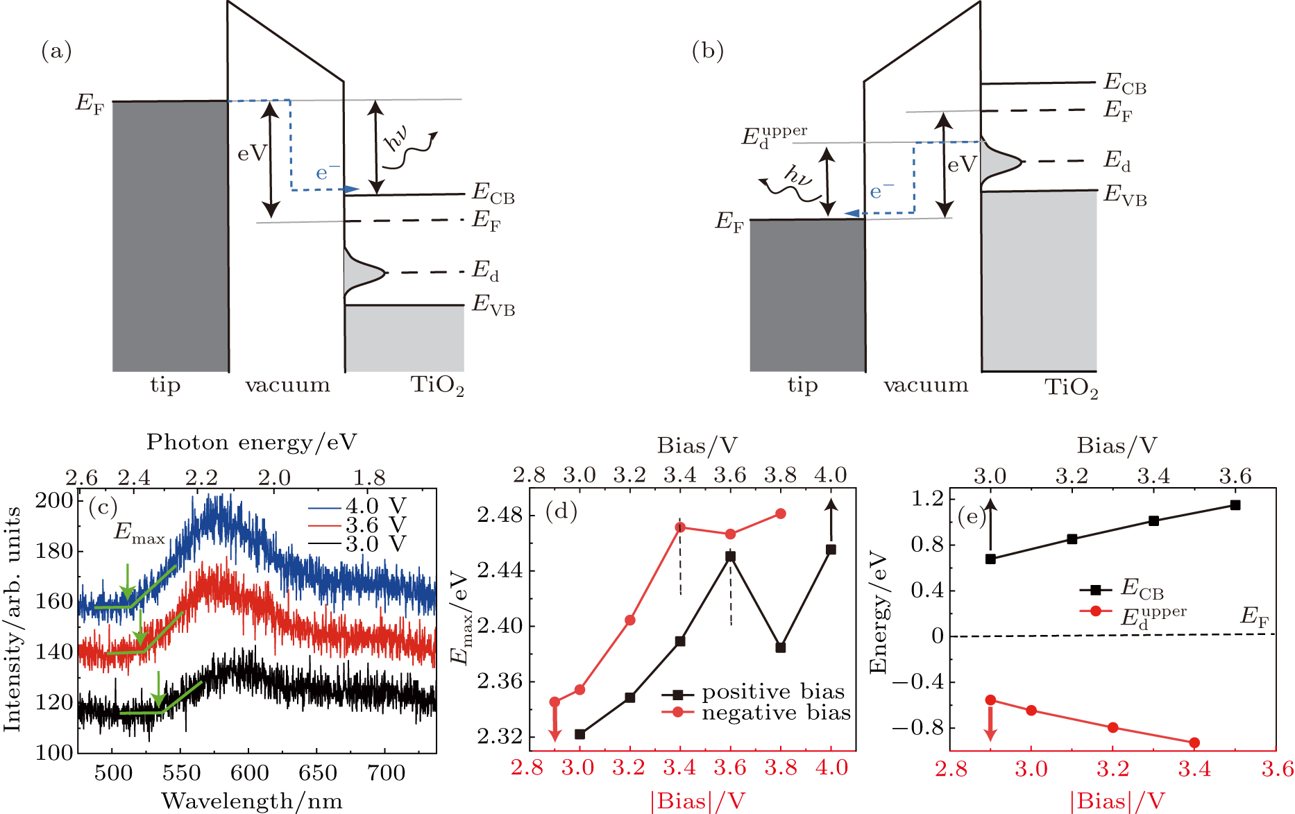
(color online) (a), (b) Energy diagrams illustrating the mechanism for light emission of TiO2(110) sample at positive and negative biases, respectively. The conduction band minimum (ECB), valence band maximum (EVB), Fermi level (EF), defect state (Ed) are indicated. The upper energy bound of defect state is denoted by Edupper . The double-headed arrows denote the sample bias (V) and the emitted photon energy (). The blue dashed line represents the inelastic tunneling processes. (c) Light emission spectra recorded at the defective TiO2(110) surface (constant-current mode, I = 3 nA, V = 3.0 V–4.0 V). The spectra are offset for clarity. The green arrows indicate the cut-off wavelengths (maximum photon energy, Emax). (d) The maximum photon energy (Emax) measured at positive (black) and negative (red) sample biases. The dashed lines mark the level-off bias voltage. (e) The energies of band edges (ECB and Edupper ) deduced from light emission spectra at positive (black) and negative (red) sample biases, respectively.