
An easy way to controllably synthesize one-dimensional SmB6 topological insulator nanostructures and exploration of their field emission applications
Cite this Article
Yang Xun, Gan Hai-Bo, Tian Yan, Xu Ning-Sheng, Deng Shao-Zhi, Chen Jun, Chen Huanjun, Liang Shi-Dong, Liu Fei. An easy way to controllably synthesize one-dimensional SmB6 topological insulator nanostructures and exploration of their field emission applications. Chinese Physics B, 2017, 26(11): 118103 
Permissions
An easy way to controllably synthesize one-dimensional SmB6 topological insulator nanostructures and exploration of their field emission applications
† Corresponding author. E-mail:
Project supported by the National Key Basic Research Program of China (Grant No. 2013CB933601), National Project for the Development of Key Scientific Apparatus of China (Grant No. 2013YQ12034506), the Fundamental Research Funds for the Central Universities of China, the Science and Technology Department of Guangdong Province, China, the Education Department of Guangdong Province, China, and the Natural Science Foundation of Guangdong Province, China (Grant No. 2016A030313313).
Abstract
A convenient fabrication technique for samarium hexaboride (SmB6) nanostructures (nanowires and nanopencils) is developed, combining magnetron-sputtering and chemical vapor deposition. Both nanostructures are proven to be single crystals with cubic structure, and they both grow along the [001] direction. Formation of both nanostructures is attributed to the vapor-liquid-solid (VLS) mechanism, and the content of boron vapor is proposed to be the reason for their different morphologies at various evaporation distances. Field emission (FE) measurements show that the maximum current density of both the as-grown nanowires and nanopencils can be several hundred μA/cm2, and their FN plots deviate only slightly from a straight line. Moreover, we prefer the generalized Schottky–Nordheim (SN) model to comprehend the difference in FE properties between the nanowires and nanopencils. The results reveal that the nonlinearity of FN plots is attributable to the effect of image potential on the FE process, which is almost independent of the morphology of the nanostructures. All the research results suggest that the SmB6 nanostructures would have a more promising future in the FE area if their surface oxide layer was eliminated in advance.
Keyword:one-dimensional SmB6 nanostructures;chemical vapor deposition (CVD);field emission (FE);image potential
1. Introduction
In recent years, nanostructures[1–8] are intensively investigated because they exhibit more fascinating properties than their bulk counterparts. Among them, SmB6 nanostructures have attracted considerable attention because they are typical Kondo topological insulators,[9–11] which are predicted to have abundant surface electronic states. But due to the anisotropy and high stability of SmB6, synthesis methods for one-dimensional SmB6 nanostructures are rather few. To our knowledge, either poisonous BCl3 gas[12] or inflammable B10H14 gas[13] is usually chosen as the boron source for recently reported synthesis of SmB6 nanowires, which inevitably implies harsh growth conditions. So it is a great challenge for researchers to find a moderate way to controllably prepare high-quality single-crystalline SmB6 nanostructures. In addition, SmB6 nanostructures may have potential applications in field emission (FE) areas because they not only have superb surface electron states but also have low electrical resistivity (2.07 × 10⁻⁴ Ω ·cm), low work function (4.4 eV), high melting point (2580 °C), and high thermal conductivity (13.8 W ·m−1·K−1).[14–17] Although some effort has been devoted to investigating their FE behaviors, the nature of their emission mechanism has not been thoroughly understood, which inhibits rapid progress in their FE applications.
In this paper, we report developing a convenient CVD method to fabricate single-crystalline SmB6 nanostructures (nanowires and nanopencils) under control. Moreover, the FE properties of the SmB6 nanowire and nanopencil films are compared in order to comprehend their intrinsic emission mechanisms. Finally, the generalized Schottky–Nordheim (SN) model is utilized to explain their different emission behaviors.
2. Experiment
The synthesis of SmB6 nanostructures was conducted in a horizontal tube-furnace by a simple low-pressure CVD method, as described in our previous publications.[2,18,19] Mixed B and B2O3 powders were used as boron sources, both of which are nontoxic and environment-friendly. They were loaded into a vessel and placed in the central region of the furnace. Sm (200 nm) and Ni (10 nm) films were respectively deposited onto the surface of Si substrate by magnetron sputtering, serving as the Sm material and catalyst of the nanostructure growth. The deposition parameters of these films are summarized in Table
X-ray diffractometry (Rigaku, D-MAX 2200 VPC) and Raman spectroscopy (Renishaw, Invia Reflex) were used to ascertain the chemical compositions of the products. The morphology and crystalline structure of the samples were respectively characterized by scanning electron microscope (SEM, Zeiss, SUPER-55) and transmission electron microscope (TEM, FEI, Titan 3 G260-300). And the FE measurements of the SmB6 nanostructure films were performed in our own custom built FE analysis and measurement system.
| Table 1. Deposition parameters for the Sm and Ni thin films. . |
3. Results and discussion
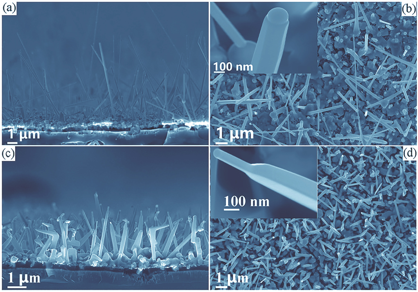
By adjusting the evaporation distance between the boron sources and the substrate, aligned SmB6 nanowires and nanopencils have been successfully fabricated on the Si substrate, respectively. SEM images of the SmB6 nanostructures are shown in Fig.
 | Fig. 1. (a), (b) Side- and top-view SEM images of the SmB6 nanowires. (c), (d) Typical morphology images of the SmB6 nanopencils. The insets are high-magnification cross-sectional images. |
| Table 2. Morphology parameters of the SmB6 nanowires and nanopencils. . |
Considering that the Ni catalysts are used in the growth process of both the SmB6 nanowires and nanopencils, we prefer to use the vapor-liquid-solid (VLS) mechanism[20] to explain the effect of the evaporation distance on the formation of different nanostructures. The possible explanations can be depicted as follows. First, the 10 nm continuous Ni film will turn into discrete catalyst nanoparticles after an hour’s pre-treatment at 700 °C. Meanwhile, some Sm atoms from the Sm film will gradually dissolve into the catalysts to form the Sm/Ni alloy nanoparticles due to their solid-state interdiffusion. Secondly, when the temperature is raised to 1000 °C, B2O2 vapor[2,21] is generated by the reaction of B and B2O3 powders, which will be transferred to the substrate region under the function of carrier gas. Third, the B2O2 vapor reacts with the Sm/Ni alloy droplets and produces the SmB6 phase with the help of the Ni catalysts. Subsequently, when the solubility of the SmB6 phase in the alloy droplets arrives at oversaturation with the proceeding of the reaction, the SmB6 solids will precipitate from the alloy droplets and form on the surface of the Si substrate, acting as the nuclei of the growth of the nanostructures. Finally, with the continuous precipitation of SmB6 from the alloy droplets, the SmB6 solid gradually forms one-dimensional nanostructures along the energy-favorable direction. Based on our analysis, two main factors must be responsible for the formation of the SmB6 nanopencils and nanowires. One is the growth temperature, because the temperature of the substrate with a 7.5 cm evaporation distance is 80 °C lower than that of the substrate with a 2.5 cm evaporation distance. As is known to us all, the lattice face vertical to the growth axis usually possesses the highest growth rate when the growth temperature is lower than a critical temperature because they have the highest surface energy. Under this circumstance, the diameter of the nanostructures decreases from the bottom to the top and the nanopencils are produced, which results from the rapid growth of the preferred face. But when the growth temperature is higher than some critical temperature, the growth speed of every lattice face tends to be equal for nanostructures, which leads to the formation of the nanowires with uniform diameter along their length. The other is the vapor pressure of the B2O2 because the evaporation distance between the source materials and the substrate is different for the formation of nanowires (3 cm) versus nanopencils (7.5 cm). With lengthening the diffusing distance of the B2O2, the vapor pressure will accordingly decrease. So this factor will also affect the formation of the SmB6 nanostructures. Moreover, our mechanism is also consistent with the growth mechanism of the LaB6 nanoobelisks[22] and ZnO nanotips.[23] So it is reasonable that the discrepancy of boron vapors at varied evaporation distances should be the intrinsic factor for the formation of different morphology of SmB6 nanostructures. The thickness of the Ni film can also affect the formation of the nanostructures. In our experiments, the thickness of the Ni film is adopted to vary from 8 nm to 15 nm. If the thickness of the Ni film is lower than 8 nm, only the SmB6 nanoparticles can be found on the substrate instead of the nanowires or nanopencils. But when the thickness of the catalysts is higher than 15 nm, the growth density of the nanostructures decreases. Therefore, the most suitable thickness of the Ni film is between 8 nm and 15 nm. The detailed mechanism is still under research.
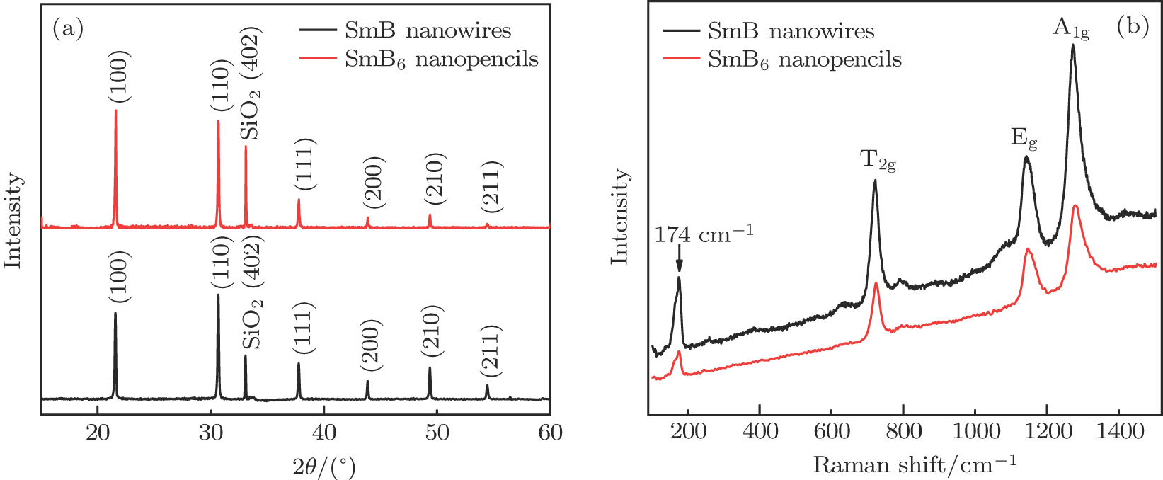
In order to confirm the chemical compositions of the as-prepared nanostructures, x-ray diffraction (XRD) and Raman spectroscopy were subsequently performed on the samples. It is found in Fig.
 | Fig. 2. (color online) (a) Typical XRD patterns and (b) Raman spectra of the SmB6 nanowires and nanopencils. |
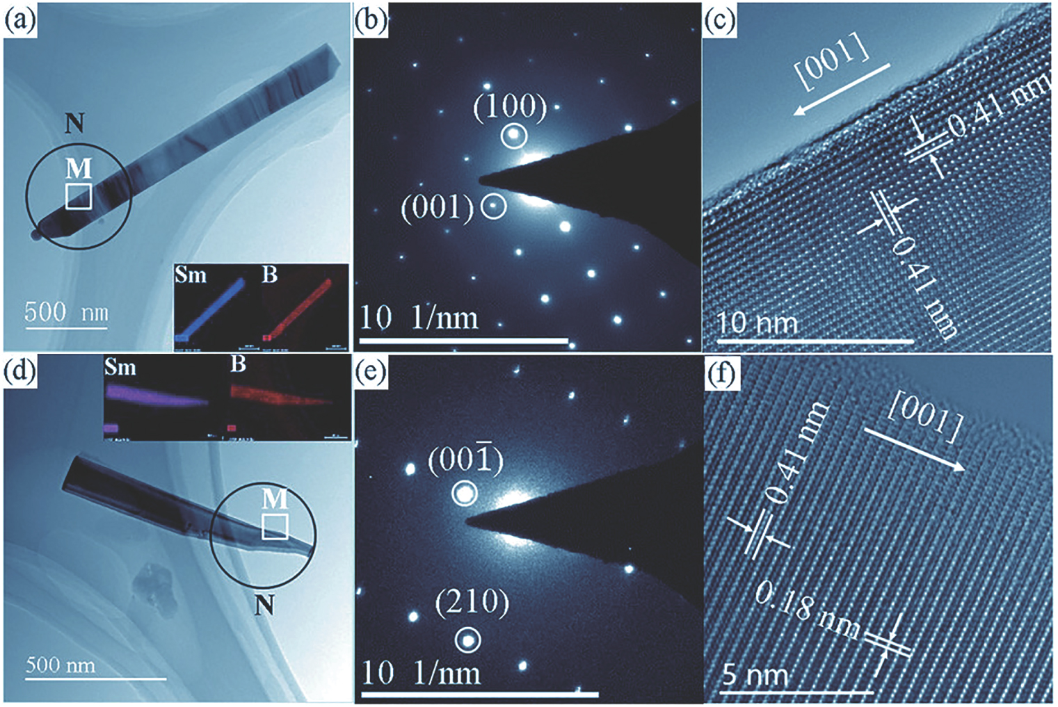
TEM images of the SmB6 nanowires and nanopencils are given in Fig.
 | Fig. 3. (color online) (a)–(c) TEM images and SAED pattern of an SmB6 nanowire. The Sm and B elemental maps are shown in the inset. (d)–(f) TEM and EDX mapping analysis of the SmB6 nanopencil. |
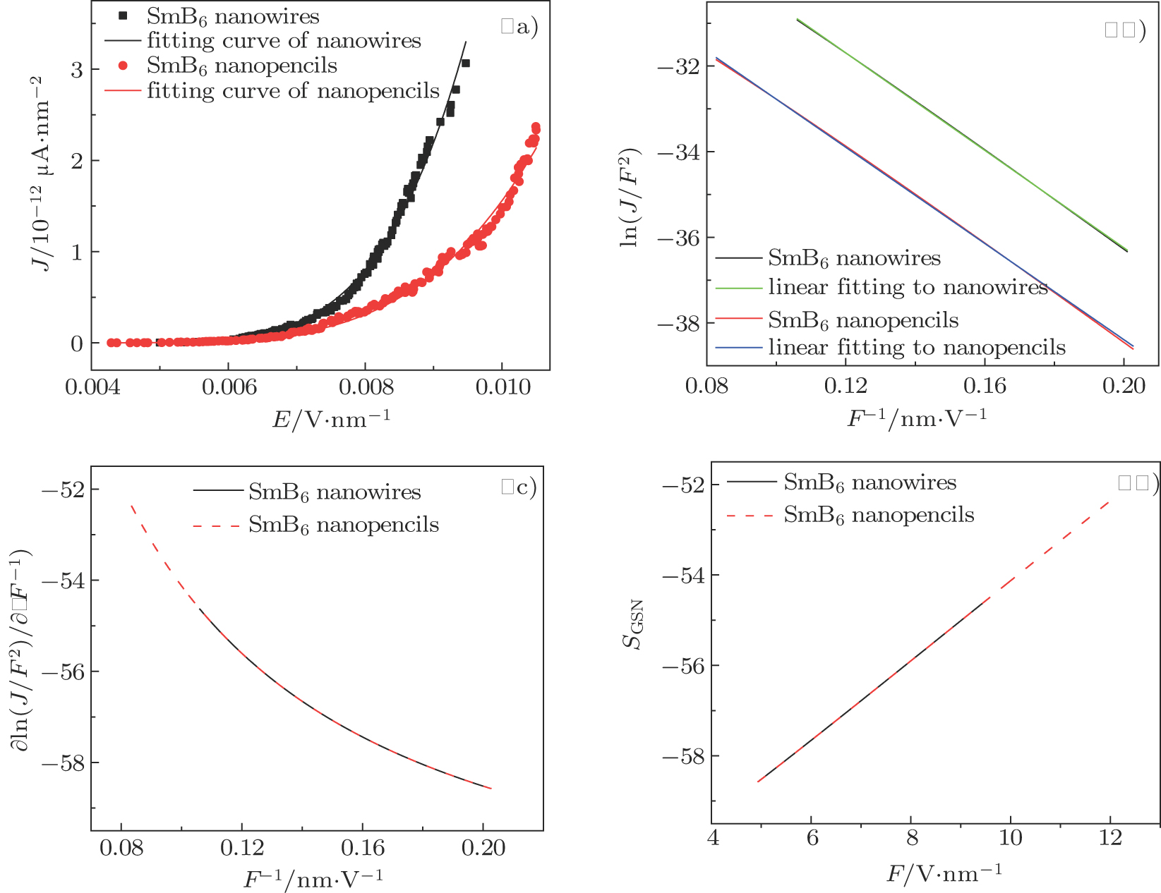
Field emission measurements of the SmB6 nanostructure film were carried out in our FE analysis and measurement system custom built in-house, in which ITO glass served as the anode. The areas of the nanowire and nanopencil films were respectively 0.49 cm2 and 0.20 cm2, and the distance between cathode and anode was kept at about 280 μm throughout the measurements. The chamber pressure was about 3.5 × 10⁻⁵ Pa and the transparent anode method was used to research on the samples. The field current density (J) versus electric field (E) curves and Fowler–Nordheim (FN) plots of the nanowires and nanopencils are shown in Figs.
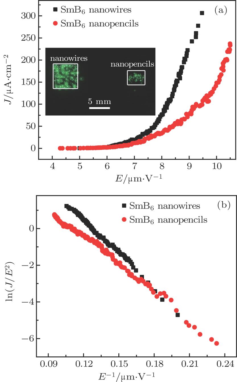 | Fig. 4. (color online) (a) FE current density-electric field (J–E) curves of the SmB6 nanowires and nanopencils. The inset shows emission images of the nanostructures. (b) The corresponding FN plots. |
In addition, it is seen in Fig.
 | Fig. 5. (color online) (a) Fitting J–E curves of the SmB6 nanostructures, (b) corresponding FN plots, (c) curves of the partial derivative of the FN plots to 1/F, (d) curves of the FN plots’ slope versus the effective electric field. |
| Table 3. Nonlinear fitting parameters of the experimental J–E curves for SmB6 nanostructures. . |
Figures
4. Conclusion
In summary, SmB6 nanostructures (nanowires and nanopencils) have been successfully fabricated on Si substrate via a convenient CVD method. Both the as-prepared SmB6 nanowires and nanopencils are indexed as single crystals with cubic structure, which grow along the [001] direction. FE measurements show that the field emission behaviors of SmB6 nanowires are better than those of SmB6 nanopencils, which may result from higher endurance under large current for the nanowires. Moreover, the generalized SN model is used to explain the nonlinear behaviors of the FN plots of the SmB6 nanowires and nanopencils, in which the effect of image potential on FE process is carefully discussed. To better exhibit the excellent emission properties of SmB6 as an ideal Kondo topological insulator, the surface oxide shell of the nanostructures must be eliminated in advance.
Reference
| [1] | |
| [2] | |
| [3] | |
| [4] | |
| [5] | |
| [6] | |
| [7] | |
| [8] | |
| [9] | |
| [10] | |
| [11] | |
| [12] | |
| [13] | |
| [14] | |
| [15] | |
| [16] | |
| [17] | |
| [18] | |
| [19] | |
| [20] | |
| [21] | |
| [22] | |
| [23] | |
| [24] | |
| [25] | |
| [26] | |
| [27] |