
Ultrafast interlayer photocarrier transfer in graphene–MoSe2 van derWaals heterostructure
Cite this Article
Zhang Xin-Wu, He Da-Wei, He Jia-Qi, Zhao Si-Qi, Hao Sheng-Cai, Wang Yong-Sheng, Yi Li-Xin. Ultrafast interlayer photocarrier transfer in graphene–MoSe2 van derWaals heterostructure. Chinese Physics B, 2017, 26(9): 097202 
Permissions
Ultrafast interlayer photocarrier transfer in graphene–MoSe2 van derWaals heterostructure
† Corresponding author. E-mail:
Project supported by the National Natural Science Foundation of China (Grant Nos. 61275058, 61527817, 61335006, and 61378073), the National Science Foundation, China (Grant No. DMR-1505852), the National Basic Research Program of China (Grant Nos. 2016YFA0202300 and 2016YFA0202302), and Beijing Science and Technology Committee, China (Grant No. Z151100003315006).
Abstract
We report the fabrication and photocarrier dynamics in graphene-MoSe2 heterostructures. The samples were fabricated by mechanical exfoliation and manual stacking techniques. Ultrafast laser measurements were performed on the heterostructure and MoSe2 monolayer samples. By comparing the results, we conclude that photocarriers injected in MoSe2 of the heterostructure transfer to graphene on an ultrafast time scale. The carriers in graphene alter the optical absorption coefficient of MoSe2. These results illustrate the potential applications of this material in optoelectronic devices
Keyword:van der Waals heterostructure;transition metal dichalcogenides;molybdenum diselenide;transient absorption
1. Introduction
The discovery of graphene in 2004[1,2] has stimulated extensive studies on its novel property and potential applications. Graphene is formed by a single layer of carbon atoms bound together in a hexagonal lattice. Due to its unique structure, graphene has many superior properties, such as high Young’s modulus and fracture strength,[3] high thermal conductivity,[4] ultrafast dynamic optical properties,[5] and high charge carrier mobility.[1] These properties make graphene an attractive candidate for various applications, such as ultracapacitors,[6,7] solar cells,[8–11] photodetector,[12] and low-power-consumption electronics.[13,14] However, the lack of a bandgap limited its application in logic electronic devices. Furthermore, its relatively small optical absorbance is also a drawback for optoelectronic applications. Monolayer transition metal dichalcogenides (TMDs), on the other hand, have remarkably high absorbance in the visible range[15] and a sizable bandgap.[16,17] However, their charge carrier mobilities are relatively low. Hence, combining graphene and TMD can potentially produce bi-layer materials that can effectively absorb light and transfer charge carriers, which are two key elements for most optoelectronic applications.
Indeed, very recently, significant progress has been made in studies of graphene–TMD heterostructures. So far, most studies have focused on combining graphene with MoS2. Initially, such heterostructures were fabricated by manually stacking graphene and MoS2 monolayers together.[18] Mechanical properties of graphene–MoS2 were studied both theoretically and experimentally.[19,20] The electronic structure of the formed heterostructure was calculated, measured, and controlled.[21–26] For electronic applications, tunneling transistors have been demonstrated with MoS2 serving as the tunneling barrier.[18,27–33] Besides these investigations on graphene–MoS2, heterostructure formed by graphene and tungsten based TMD monolayers has also been studied. For graphene–WS2, spin–orbit interaction[34] and various applications have been attempted, such as tunneling transistors,[29,35] photovoltaics,[36] light-emitting diodes,[37] and photodetection.[38] Measurements of its band alignment,[39] photoluminescence properties,[40] and light-emitting devices[37] have been reported.
In contrast to these extensive efforts on developing heterostructures formed by graphene and MoS2 and WS2, MoSe2 has been seldom used to form heterostructures with graphene. The only reports on graphene–MoSe2 heterostructures are their molecular beam expitaxy[41] and observation of photoluminescence quenching.[42] MoSe2 possesses several properties that make it an attractive member of TMDs. It has a direct optical bandgap of 1.55 eV,[43] which is near the optimal bandgap of single-junction photovoltaic devices and photocatalysis.[44–46]
Here we report fabrication of graphene–MoSe2 heterostructures and ultrafast laser measurements on photocarrier dynamics. We observed efficient carrier transfer from MoSe2 to graphene, and strong effect of carriers in graphene on optical properties of MoSe2. These results indicate that graphene–MoSe2 heterostructures are promising materials for optoelectronic applications.
2. Experiment
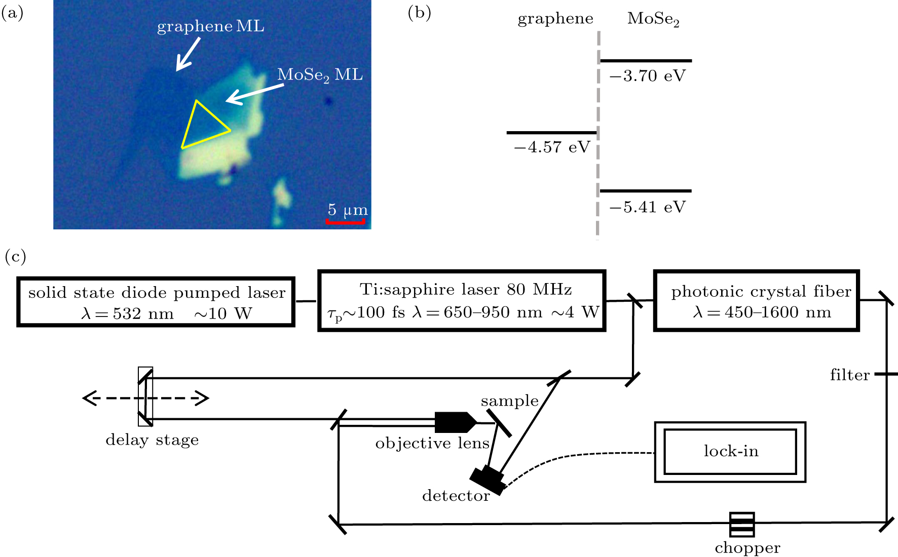
Graphene and MoSe2 flakes were fabricated by mechanical exfoliation. Adhesive tapes were used to mechanically exfoliate flakes from bulk crystals onto polydimethylsiloxane (PDMS) substrates. The monolayers were identified by optical contrasts with an optical microscope. Then a MoSe2 monolayer flake was transferred to a Si substrate with a 90 nm SiO2 layer and annealed for 2 h at 200 °C in an Ar (60 sccm) environment with a pressure of 3 Torr. Next, a graphene flake was transferred onto the MoSe2 flake, followed by the same annealing procedure. The final optical microscope image of the sample is shown in Fig.
 | Fig. 1. (color online) (a) Microscope images of the samples studied. (b) Band alignment of graphene and MoSe2 monolayers. (c) Experimental setup to measure differential reflectivity. |
In the transient absorption microscopy setup shown as Fig.
3. Results and discussion
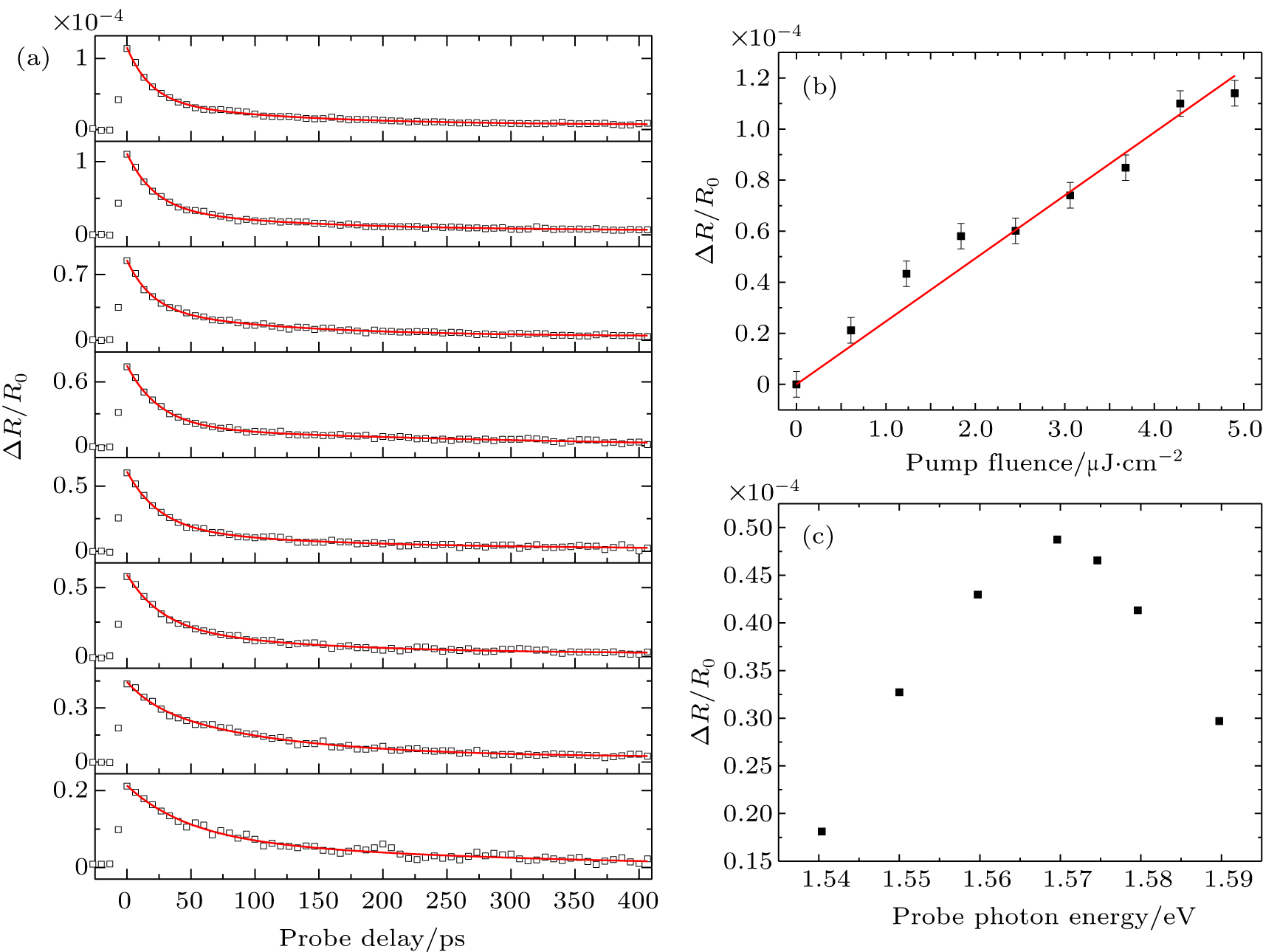
We first studied a MoSe2 monolayer sample. A pump pulse of 2.00 eV was used to inject photocarriers. A probe pulse of 1.57 eV, which is tuned near to the exciton resonance of MoSe2, was used to monitor these photocarriers. The top panel of Fig.
 | Fig. 2. (color online) Differential reflectivity measurement of monolayer MoSe2. (a) Differential reflectivity signal as a function of probe delay with pump fluences of (from top to bottom) 4.9, 4.29, 3.06, 2.45, 1.84, 1.23 and 0.61 μJ/cm2, respectively. The red curves are exponential fits. (b) Peak differential reflectivity signal as a function of pump fluence. (c) Peak differential reflectivity signal as a function of the probe photon energy. |
Figure
Figure
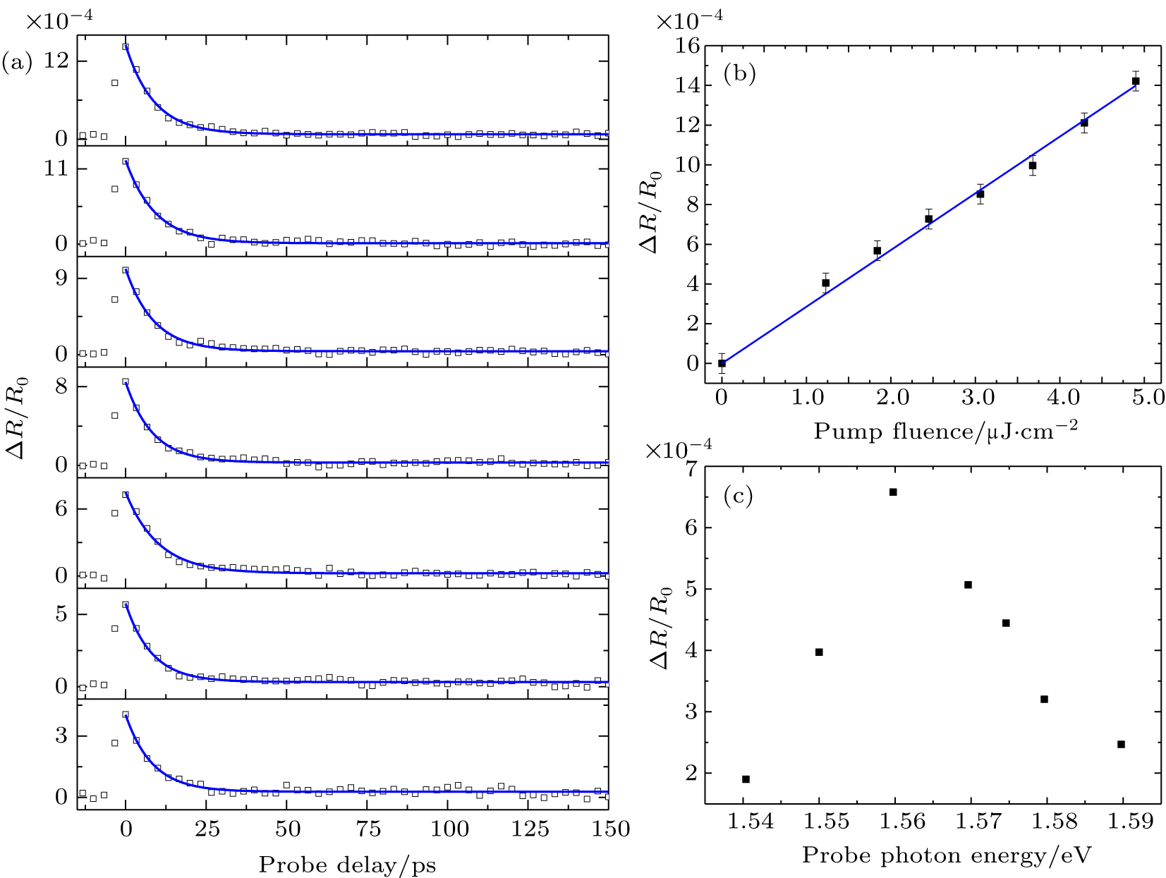 | Fig. 3. (color online) Differential reflectivity measurement of graphene–MoSe2 heterostructure. (a) Differential reflectivity signal as a function of probe delay with pump fluences of (from top to bottom) 4.9, 4.29, 3.06, 2.45, 1.84 and 1.23 μJ/cm2, respectively. The blue curves are exponential fits. (b) Peak differential reflectivity signal as a function of pump fluence. (c) Peak differential reflectivity signal as a function of the probe photon energy. |
We attribute these observed features to two physical mechanisms. First, the photocarriers excited in MoSe2 rapidly transfer to graphene. Second, the carriers in graphene can induce a differential reflectivity signal of the probe tuned to the MoSe2 resonance.
The strong dependence of the peak signal on probe photon energy indicates that the signal originates from a change of the absorption coefficient of MoSe2. However, this change cannot be induced by the photocarriers in MoSe2, since in the measurements on MoSe2 monolayer (Fig.
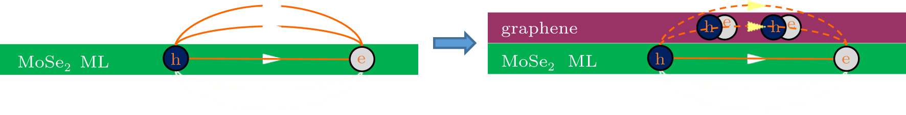
We assume that the mechanism for change of the absorption coefficient of MoSe2 by carriers in graphene is via a screening effect of these carriers on the electric field of the excitons. It has been well established that the Coulomb interaction between electrons and holes in monolayer TMDs is significantly enhanced by the reduced dielectric screening. As shown in Fig.
 | Fig. 4. The electric field of the excitons in MoSe2 before and after forming the heterostruture. |
Therefore, our results provide quantitative information on the physics mechanism of screening of graphene on many-body interactions in MoSe2 monolayers. In particular, it is possible to control the electron–hole interaction in MoSe2, as well as other 2D materials, by interfacing with graphene with a certain thickness. This opens up the opportunities of controlling electron–hole interactions in van der Waals materials.
Based on this mechanism and the fast decay of the signal observed in Fig.
The observed effects have important implications on using these materials in optoelectronic devices. For example, the efficient transfer of photocarriers from MoSe2 to graphene suggests that such bilayers can be used in photodetectors and solar cells. MoSe2 has a large absorption coefficient at optimal wavelength for solar cells, while graphene possesses superior charge transport performance. The bilayer structure effectively combines these advantages. The demonstrated control of MoSe2 absorption by carriers in graphene can be utilized in light modulation applications where gate controlled carriers in graphene can be used to modulate absorption of light by MoSe2.
4. Conclusion
We have fabricated a less investigated graphene–MoSe2 heterostructure, and studied its photocarrier dynamics. We found that photocarriers injected in MoSe2 transfer to graphene on an ultrafast time scale. We also found that a carrier in graphene can change the excitonic absorption of MoSe2, which can be potentially used for electric control of optical absorption of MoSe2. Our results illustrate that graphene–MoSe2 heterostructures can effectively combine the novel optical absorption property of MoSe2 and charge the transport property of graphene, for potential applications in optoelectronic devices.
Reference
| [1] | |
| [2] | |
| [3] | |
| [4] | |
| [5] | |
| [6] | |
| [7] | |
| [8] | |
| [9] | |
| [10] | |
| [11] | |
| [12] | |
| [13] | |
| [14] | |
| [15] | |
| [16] | |
| [17] | |
| [18] | |
| [19] | |
| [20] | |
| [21] | |
| [22] | |
| [23] | |
| [24] | |
| [25] | |
| [26] | |
| [27] | |
| [28] | |
| [29] | |
| [30] | |
| [31] | |
| [32] | |
| [33] | |
| [34] | |
| [35] | |
| [36] | |
| [37] | |
| [38] | |
| [39] | |
| [40] | |
| [41] | |
| [42] | |
| [43] | |
| [44] | |
| [45] | |
| [46] | |
| [47] | |
| [48] | |
| [49] | |
| [50] |