Electronic structure and nematic phase transition in superconducting multiple-layer FeSe films grown by pulsed laser deposition method
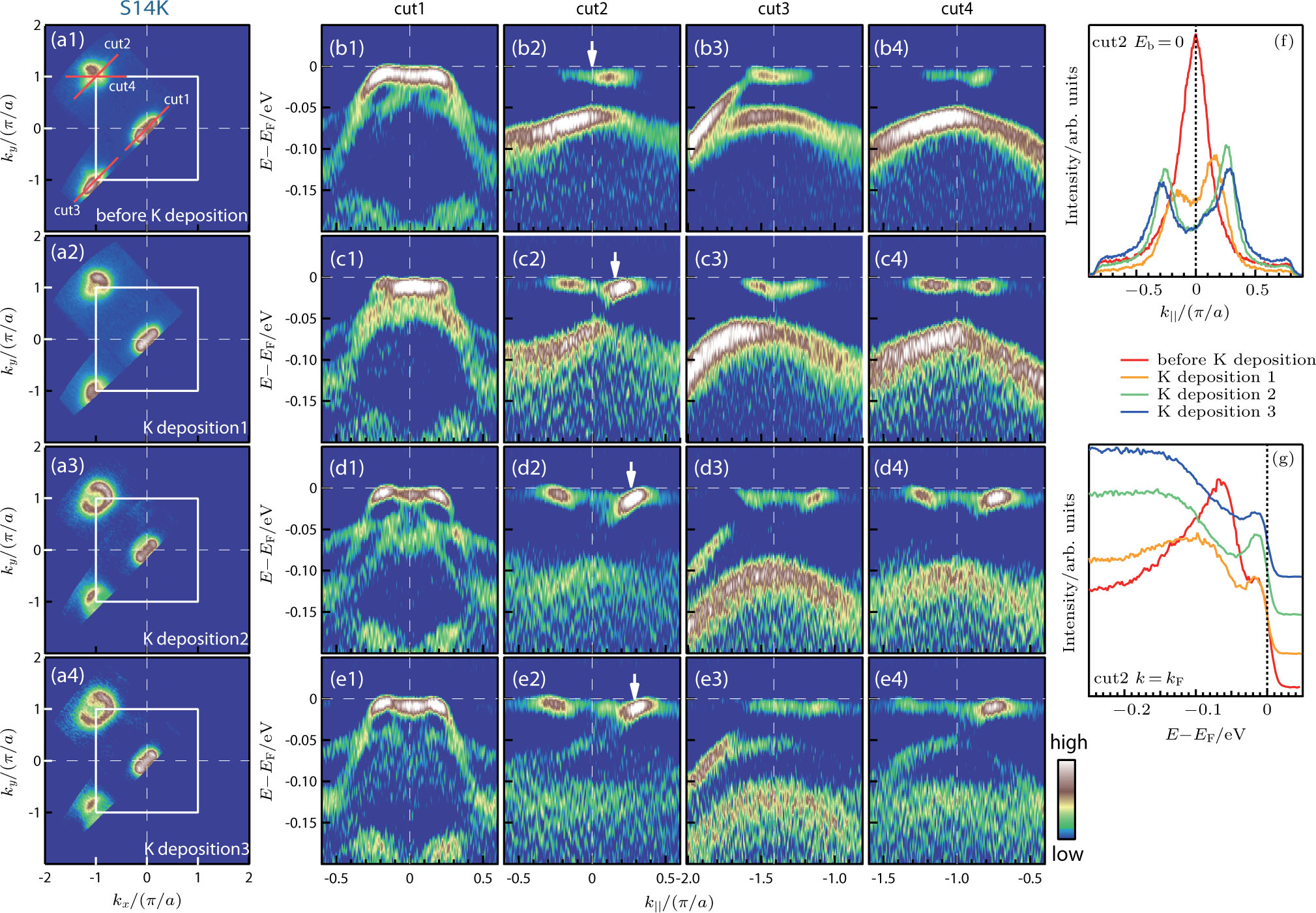
Fermi surface and band structure of the S14K sample measured at 30 K before and after potassium deposition. (a1) show Fermi surface mapping before potassium deposition, and (a2)–(a3) show Fermi surface mapping after three consecutive potassium depositions. They are obtained by integrating the spectral weight with [−20 meV, 10 meV] energy window with respect to the Fermi level. (b1)–(b4) show band structure measured for the sample before potassium deposition along four momentum cuts; their locations are marked in (a1) as red lines. (c1)–(c4), (d1)–(d4), and (e1)–(e4) show band structure along the four momentum cuts after three consecutive potassium depositions. These images are obtained by taking second derivatives with respect to energy on the original data. (f) shows the MDCs at the Fermi level for the cut crossing M2 point (cut 2) before K deposition and after three K depositions. (g) shows the EDCs at the Fermi momentum