Asymmetrical plasmon reflections in tapered graphene ribbons with wrinkle edges
Yang Cui1, 2, Chen Runkun1, 2, Jia Yuping1, 2, 4, Guo Liwei1, 2, †, Chen Jianing1, 2, 3, ‡
Beijing National Laboratory for Condensed Matter Physics, Institute of Physics, Chinese Academy of Sciences, Beijing 100190, China
School of Physical Sciences, University of Chinese Academy of Sciences, Beijing 100049, China
Collaborative Innovation Center of Quantum Matter, Beijing 100190, China
Changchun Institute of Optics, Fine Mechanics and Physics, Chinese Academy of Sciences, Changchun 130033, China


† Corresponding author. E-mail: lwguo@iphy.ac.cn jnchen@iphy.ac.cn

Abstract

Asymmetrical graphene plasmon reflection patterns are found in infrared near-field images of tapered graphene ribbons epitaxially grown on silicon carbon substrates. Comparing experimental data with numerical simulations, the asymmetry of these patterns is attributed to reflection of plasmons by wrinkled edges naturally grown in the graphene. These graphene wrinkles are additional plasmon reflectors with varying optical conductivity, which act as nanometer scale plasmonic modulators and thus have potential applications in photoelectric information detectors, transmitters, and modulators.

1. Introduction

Graphene is a one-atom-thick carbon material, with carbon atoms packed densely in a hexagonal honeycomb lattice. Having a unique energy band structure, graphene also has tunable optical and electronic performance, which attracts great interest in electronics and plasmonics and can be used in fabricating photoelectric devices such as polarizers, absorbers, and so on.[18] Graphene also has semimetal properties, so the existence of graphene plasmon has long been predicted in theory. Based on experiments with scattering-type scanning near-field microscopy (s-SNOM), we know that graphene plasmons can be excited by a metallic atomic force microscope tip illuminated with light from infrared to terahertz frequency and propagate on the graphene. The real-space imaging of graphene plasmons is possible because of the formation of standing waves coming from the interference between the tip-launched plasmons and the plasmons reflected back by graphene edges, defects, boundaries, or substrate steps.[912]

Graphene plasmon has a shorter wavelength than excitation illumination in the IR region, by about 1/20, and it has a stronger localized electromagnetic field than its counterparts among noble metals.[9,10] Graphene plasmons are sensitive to surface topological features and form various interference patterns in the near field.[13,14] Fei et al. reported distinct plasmon interference patterns in a tapered graphene ribbon.[13] Fang et al. demonstrated tunability and hybridization of localized plasmon in nanostructured graphene.[15] Nikitin et al. performed a detailed near-field optical modes study on graphene disks and rectangular nano-resonators.[14] Graphene edges and other defects are naturally-grown plasmon scatters that affect graphene plasmonic modes.[16,17] Martin-Moreno et al. theoretically investigated the scattering of graphene plasmon by atomic level defects in graphene sheets.[17] Fei et al. showed that local electronic properties in graphene can be revealed by analyzing the corresponding local plasmonic interference patterns.[12]

In the present paper, we report our near-field infrared imaging study of the asymmetrical plasmon interference patterns found on tapered graphene ribbons with wrinkled edges. Graphene wrinkles exhibit a dual-function reflection effect on plasmons. It is found that the topological shape of the wrinkles alone has little effect on plasmon propagation, and the varied conductivity of the wrinkles gives rise to plasmon reflections at graphene wrinkles. When graphene wrinkles appear at the edges, they can be regarded as a perturbative factor for plasmon reflection, leading to unusual asymmetrical plasmon interference patterns in the near field. Graphene wrinkles with changed optical conductivities can be potentially used as tuneable plasmonic scatterers for manipulating light at the nanometer scale.[18]

2. Materials and methods

Tapered graphene ribbons are grown on SiC (11-20) by a thermal decomposition method.[7,19] At the growth temperature, graphene first begins nucleation on the SiC surface, then extends to form tapered graphene ribbons quickly. After graphitization, we lower the temperature to room temperature, whereupon wrinkles appear in the graphene ribbons to release compressive stress that exists in the graphene ribbons because the thermal expansion coefficients of graphene and SiC differ. A detailed Raman characterization of the graphene grown on SiC is shown in Fig. S1.

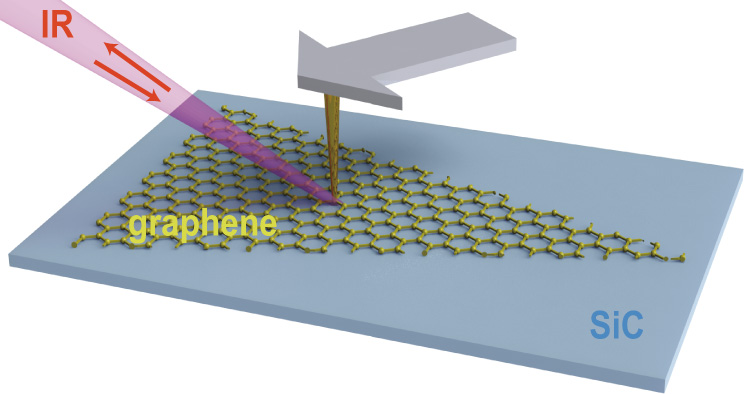
A schematic of scattering-type scanning near-field optical microscopy on tapered graphene ribbons is shown in Fig. 1. The atomic force microscope (AFM) metal tip is illuminated by an infrared light of wavelengths tunable from 9 μm to 11 μm. The tip compensates the momentum mismatch between photons and plasmons, which launches propagating graphene plasmons. The interference surface standing wave between the propagating plasmon and the reflected plasmon is scattered by the same tip to the far field and recorded by an infrared detector. To suppress background noise, a pseudo-heterodyne interferometric detection scheme is employed, providing background-free third-harmonic near-field images for study.[11]

Fig. 1. (color online) Schematic of scattering-type scanning near-field optical microscopy. The excitation light is an infrared laser, and the sample is epitaxially grown graphene on silicon carbon substrate.
3. Results and discussion

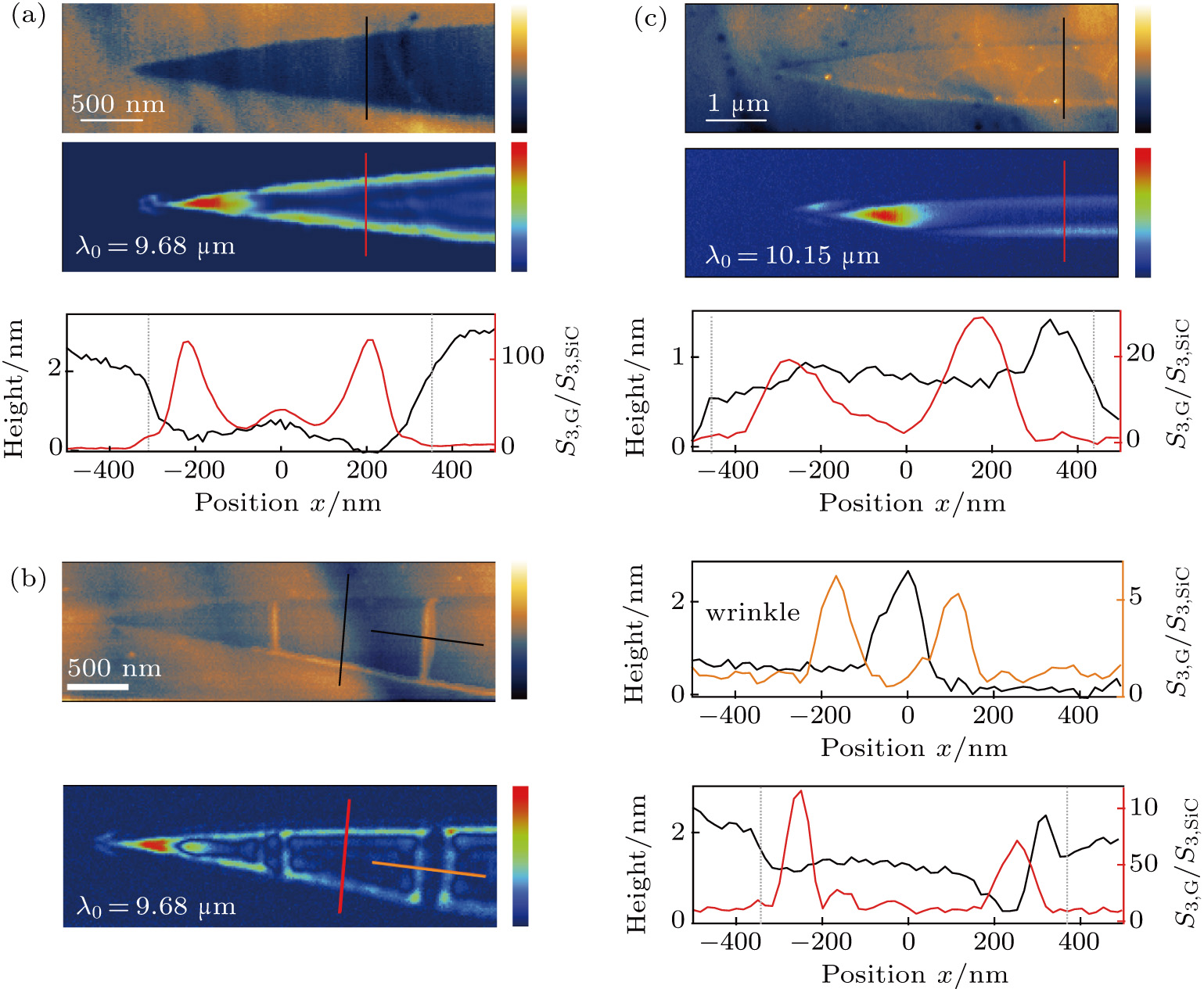
The near-field optical and corresponding topological images of the tapered graphene ribbons are shown in Fig. 2. For the monolayer graphene ribbon, there is a symmetry near-field optical pattern with a similar signal strength at two edges, which is shown as the red profile line in Fig. 2(a). Figure 2(b) shows graphene wrinkles inside and at the edges of the graphene ribbons. These wrinkles can reflect graphene plasmons. The horizontal orange line in the optical image of Fig. 2(b) shows a graphene wrinkle inside a graphene ribbon, and the vertical red line in the optical image of Fig. 2(b) shows a graphene wrinkle at the bottom side of a graphene ribbon. The corresponding profiles are plotted in the right panel of Fig. 2(b). For the red profiles in the bottom right panel of Fig. 2(b), the near-field optical signal is weaker at the wrinkle edges on the right side, which indicates that graphene wrinkles at the graphene edge modify its local optical conductivity and, consequently, modify the plasmon reflection ratio there.

Fig. 2. (color online) Optical nano-imaging of graphene ribbons. (a) Upper panel: topological image of a graphene ribbon; middle panel: near-field image; lower panel: topological and near-field signal profiles extracted from the above images, with positions indicated by the black line in the topological image and the red line in the near-field image, respectively. The scale bar is 500 nm and the wavelength of incident light is 9.68 μm. (b) Left: topological and near-field images of graphene ribbon with wrinkles in the top and bottom panels, respectively; right panels: topological and near-field signal profiles extracted from the left. The topological profile is indicated by the black line, and the optical signal profiles are indicated by the red and orange lines in the near-field image. The scale bar is 500 nm and the wavelength of incident light is 9.68 μm. (c) Upper panel: topological image of a graphene ribbon; middle panel: near-field optical imaging; lower panel: the topological and near-field signal profiles are indicated by the black line in the topological image and the red line in the optical image, respectively. The scale bar is 1 μm and the incident wavelength is 10.15 μm.

In Fig. 2(c), we show other plasmons reflected by wrinkled graphene edges. The intensity pattern of the optical near-field image is asymmetric, i.e., the optical signal is stronger at one wrinkled edge side than at the other, in contrast with the case shown in Fig. 2(b). This suggests that the plasmon reflection ratio at a wrinkled edge is a joint effect of wrinkles and edges, and wrinkles at graphene edges can either enhance or weaken plasmon reflection, depending on the individual case. In order to understand our experimental results well and quantify the effect of graphene wrinkles on graphene plasmon reflection, we employ numerical calculations (Comsol, wave optics module) to simulate graphene plasmon reflection at graphene edges, wrinkles, and their synergetic effects.

In the simulation model, the role of the scanning AFM metal tip in the experiment is replaced by a vertically oriented dipole to excite a graphene plasmon. Graphene is modeled as a surface current with . The optical conductivity of graphene is derived by the random phase approximation method.[9] In the model, the dipole scans above the graphene surface, and a point detector simultaneously records the electric field at about 30 nm below the dipole. By deducting a constant background signal, the calculated electrical field intensity profile can be directly compared with our experimental results.[11]

First, we calculate the edge reflection effects of plasmon propagation, as shown in Fig. 3. A schematic of graphene edges is shown in Fig. 3(a). The graphene is illuminated with a 10.00 μm laser and the grey dashed line marks the edge position. The zero point of the position is defined at the center of SiC. The calculated near-field profiles change with varying graphene Fermi energy , as shown in Fig. 3(b). The signal profile is normalized with the intensity of SiC. We define the signal difference between the maximum peak value of the interference near-field profile and the value of flat graphene as . It is found that it is nearly constant, independent of graphene doping concentrations, as shown in the inset of Fig. 3(b).

Fig. 3. (color online) Simulation results of graphene edge reflection only. (a) Schematic figure of graphene edges. (b) Near-field optical signal profile across the edge for different Fermi energy. The inset is the signal difference between the maximum peak value and the intensity of flat graphene from the interference near-field profile, which shows a stable reflection effect that is independent of the Fermi energy.

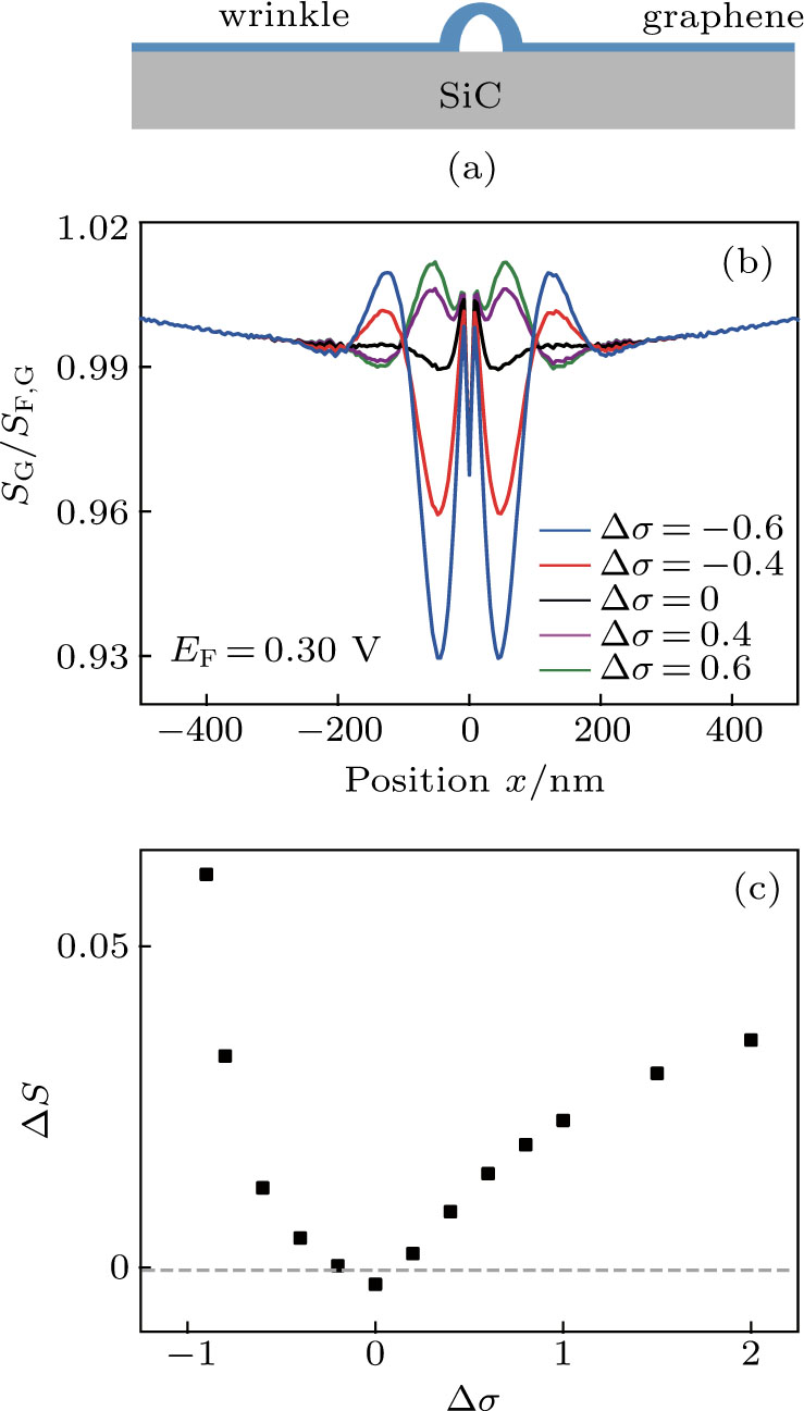
Wrinkle defects in graphene introduce a different reflection effect for plasmons.[20] The calculation model is shown in Fig. 4(a). By deducing the topological convolution of the effects of the AFM tip and the graphene wrinkles, we find that a graphene wrinkle has a Gaussian spatial profile with a height of almost 2 nm and a width of about 30 nm. The modified plasmon reflection effect induced by the topological shape of a graphene wrinkle alone is weak (the black line in Fig. 4(b)). The experimental results in Fig. 2 show a clear difference in plasmon reflection that is attributable to wrinkled edges. Therefore, it is inferred that this dominant discrepancy is caused by varying optical conductivity at the wrinkle's position. Here, the position x = 0 represents the center position of a graphene wrinkle.[17] The modeled conductivity profile of graphene wrinkles resembles the geometric wrinkle curvatures. We designate the optical conductivity difference as , where and are the optical conductivity at a wrinkle position and in flat grapheme, respectively. The induced plasmon reflection appears both in the increased and decreased optical conductivity cases at graphene wrinkles, as shown in Fig. 4(b). In the case of increased optical conductivity at a graphene wrinkle (), two fringes appear, one at each side of the wrinkle. Comparing our experimental results in Fig. 2(b) with our simulation results, it is deduced that for a wrinkle inside a graphene ribbon, . For the case of decreased optical conductivity (), the near-field profile includes peaks in the center of the graphene wrinkle in addition to the two fringes outside the wrinkle, which is caused by multiple plasmon reflections arising from the varying conductivity at the graphene wrinkle. Movement of the peak positions of the fringes on the sides of the graphene wrinkle is caused by a different plasmon reflection phase delay, also arising from the varying optical conductivity at wrinkles.

Fig. 4. (color online) Simulated near-field optical profiles at graphene wrinkles. (a) Schematic of graphene wrinkles on flat graphene. (b) Near-field optical signal profiles of graphene wrinkles with different optical conductivities at a wrinkle position. Wrinkles with increased or decreased optical conductivity give different line shapes. (c) Signal difference between the maximum peak value of the interference fringe and the flat graphene with different optical conductivities.

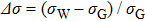
In a further step, we numerically calculate the case of plasmon reflection taking place at wrinkled graphene edges, which necessarily considers the synergetic plasmon reflection effects of graphene edges and wrinkles. A schematic of the calculation model is shown in Fig. 5(a): the left side represents a normal graphene edge and the right side models a wrinkled graphene edge. If only the topological shape of the graphene wrinkle is considered and other conditions are kept identical, the calculated near-field optical profile of this case is symmetrical, which means that the wrinkled shape alone does not affect plasmon reflection differently compared to the normal graphene edge (the black line in Fig. 5(b)). When the optical conductivity of the wrinkled edge is increased, there is no obvious change in the interference profile of the normal edge, but the near-field signal strength of the wrinkled edge's fringe becomes slightly stronger than the normal edge. While with decreased optical conductivity at a graphene wrinkle edge, the corresponding signal strength becomes lower than that of the normal edge. Also, the Fermi energy of the graphene ribbons and the substrates have some influence on plasmon reflection patterns, as shown in Figs. S2 and S3. In Fig. 2(b), the weaker near-field optical signal strength occurring at wrinkled edges may be attributable to the detachment from the substrate, which leads to a weak doping from the substrate at the wrinkle, consistent with our simulation of decreased conductivity in the wrinkled edge. On the other hand, figure 2(c) shows stronger plasmon reflection at the wrinkle edge, which may be due to adsorption of molecules from the air onto the wrinkle and edge, resulting in slightly increased optical conductivity in the wrinkle. Both of these cases are qualitatively consistent with our simulations. Quantitatively, we define to represent the different reflection effects of edges and wrinkled edges, as given in Fig. 5(c), where and are the maximum peak values of a edge and a wrinkled edge, respectively. Figure 5(c) clearly shows that decreasing optical conductivity in a wrinkle contributes a more prominent effect on the reflection intensity than increasing conductivity does, which can certainly be used to tailor plasmon propagation at wrinkles.

Fig. 5. (color online) Simulation results of wrinkled graphene edges. (a) Schematic of wrinkled graphene edges. (b) Near-field optical signal profiles of graphene ribbons with different optical conductivity at wrinkle positions. The left edge side has a fixed signal strength, while the near-field optical profile of the wrinkled edges differs, with varying optical conductivity at graphene wrinkles. (c) Signal difference between the right peak and the left peak of reflection fringes with varying optical conductivity at graphene wrinkles.
4. Conclusion and perspectives

Graphene wrinkles located either inside or at edges strongly reflect and modulate plasmons. Especially, wrinkled edges of graphene ribbons serve the usual functions of a physical edge in two dimensions while also changing the optical conductivity to modulate graphene plasmons. Concretely, increasing or decreasing optical conductivity at wrinkles inside a graphene ribbon introduces an extra reflection effect with comprehensive phase and amplitude interference. At the edges, introducing wrinkles changes the optical conductivity, contributing another regime. When > 0, the effect of superposing wrinkles is a weak increase in reflection. While for < 0, a sharply decreased plasmon reflection signal is observed, indicating weaker plasmon reflection at wrinkle edges. These results indicate that graphene plasmons are sensitive to local optical conductivity variations, a phenomenon which can be extended to probe and evaluate the electronic properties of different defects. On the other hand, these local surface defects can be used to modify plasmons for local electric field enhancement at the nanometer scale in the infrared region.

Reference
[1] Avouris P 2010 Nano Lett. 10 4285
[2] García de Abajo F J 2014 ACS Photon. 1 135
[3] Yang X X Kong X T Dai Q 2015 Acta. Phys. Sin. 64 106801 in Chinese
[4] Politano A Chiarello G 2014 Nanoscale 6 10927
[5] Bao Q Zhang H Wang Y Ni Z Yan Y Shen Z X Loh K P Tang D Y 2009 Adv. Funct. Mater. 19 3077
[6] Bao Q Zhang H Wang B Ni Z Lim C H Y X Wang Y Tang D Y Loh K P 2011 Nat. Photon. 5 411
[7] Jia Y Guo L Lu W Guo Y Lin J Zhu K Chen L Huang Q Huang J Li Z Chen X 2014 Sci. China Phys. Mech. 56 2386
[8] Fang Z Wang Y Schlather A E Liu Z Ajayan P M de Abajo F J Nordlander P Zhu X Halas N J 2014 Nano Lett. 14 299
[9] Chen J Badioli M Alonso-Gonzalez P Thongrattanasiri S Huth F Osmond J Spasenovic M Centeno A Pesquera A Godignon P Elorza A Z Camara N Garcia de Abajo F J Hillenbrand R Koppens F H 2012 Nature 487 77
[10] Fei Z Rodin A S Andreev G O Bao W McLeod A S Wagner M Zhang L M Zhao Z Thiemens M Dominguez G Fogler M M Castro Neto A H Lau C N Keilmann F Basov D N 2012 Nature 487 82
[11] Chen J Nesterov M L Nikitin A Y Thongrattanasiri S Alonso-Gonzalez P Slipchenko T M Speck F Ostler M Seyller T Crassee I Koppens F H Martin-Moreno L Garcia de Abajo F J Kuzmenko A B Hillenbrand R 2013 Nano Lett. 13 6210
[12] Fei Z Rodin A S Gannett W Dai S Regan W Wagner M Liu M K McLeod A S Dominguez G Thiemens M Castro Neto A H Keilmann F Zettl A Hillenbrand R Fogler M M Basov D N 2013 Nat. Nanotechnol. 8 821
[13] Fei Z Goldflam M D Wu J S Dai S Wagner M McLeod A S Liu M K Post K W Zhu S Janssen G C Fogler M M Basov D N 2015 Nano Lett. 15 8271
[14] Nikitin A Y Alonso-González P Vélez S Mastel S Centeno A Pesquera A Zurutuza A Casanova F Hueso L E Koppens H L Hillenbrand R 2016 Nat. Photon. 10 239
[15] Fang Z Thongrattanasiri S Schlather A Liu Z Ma L Wang Y Ajayan P M Nordlander P Halas N J Garcia de Abajo F J 2013 ACS Nano 7 2388
[16] Banhart F Kotakoski J Krasheninnikov A V 2011 ACS Nano 5 26
[17] Garcia-Pomar J L Nikitin A Y Martin-Moreno L 2013 ACS Nano 7 4988
[18] Schedin F Geim A K Morozov S V Hill E W Blake P Katsnelson M I Novoselov K S 2007 Nat. Mater. 6 652
[19] Jia Y Guo L Lin J Yang J Chen X 2017 Carbon 114 585
[20] Jia Y P Guo L W Li Z L Huang J Lu W Chen H X Chen X L 2016 Adv. Electron. Mater. 2 1500255