Transparent conducting indium-tin-oxide (ITO) film as full front electrode in III–V compound solar cell
Dai Pan, Lu Jianya, Tan Ming, Wang Qingsong, Wu Yuanyuan, Ji Lian, Bian Lifeng, Lu Shulong, Yang Hui
Key Laboratory of Nanodevices and Applications, Suzhou Institute of Nano-Tech and Nano-Bionics, Chinese Academy of Sciences (CAS), Suzhou 215123, China


† Corresponding author. E-mail: sllu2008@sinano.ac.cn

Abstract

The application of transparent conducting indium-tin-oxide (ITO) film as full front electrode replacing the conventional bus-bar metal electrode in III–V compound GaInP solar cell was proposed. A high-quality, non-rectifying contact between ITO and 10 nm -GaAs contact layer was formed, which is benefiting from a high carrier concentration of the terrilium-doped -GaAs layer, up to 2 . A good device performance of the GaInP solar cell with the ITO electrode was observed. This result indicates a great potential of transparent conducting films in the future fabrication of larger area flexible III–V solar cell.

1. Introduction

III–V compound multi-junction solar cells have been extensively researched and achieved ultrahigh conversion efficiency due to their wide spectral absorption of solar energy.[13] Numerous studies have been conducted with different epitaxial growth techniques and differently designed device structures to improve their performances.[46] To reduce the shadow loss and to increase the current extraction capability, the transparent conducting film was proposed to replace bus-bar metals in the III–V compound solar cells as the new electrode.[7]

The indium-tin-oxide (ITO) film has been widely utilized as the transparent conducting electrode in various optoelectronic devices because of its excellent electrical and optical properties.[810] However, it is difficult to form good ohmic contact between ITO film and III–V semiconductor. In addition, the specific resistance of the ITO film is higher than that of the AuGeNi/Au metal normally used for the III–V compound solar cells.[11] Therefore, a hybrid electrode structure consisting of metal contact pads and ITO films is universally employed to enhance the device performance.[12,13] But such a hybrid structure increases the complexity of the device fabrication procedure. An easy way to fabricate the device with only ITO as the electrode is therefore highly anticipated.[14,15]

In this paper, we propose the application of transparent conducting ITO film as the new full front electrode to replace the conventional bus-bar metals in the III–V compound GaInP solar cell. The ITO film effectively transports carriers in a way similar to the bus-bar of the conventional metal electrode. By inserting a 10 nm highly Te-doped -GaAs between ITO and AlInP window layer, a high-quality non-rectifying contact between ITO and 10 nm -GaAs contact layer was formed. The successful operation of the full ITO electrode not only simplifies the device fabrication process, but also gives great promise to the future application of transparent conducting films in larger area flexible III–V solar cell fabrication.

2. Experiments

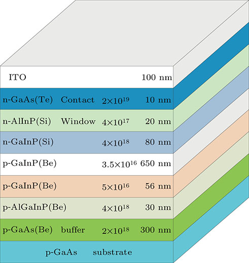
The epitaxial material of the GaInP solar cell was grown on a p-type GaAs substrate by all solid-state molecular beam expitaxy (MBE). The structure of the GaInP solar cell grown on the p-type GaAs substrate includes a p-GaInP base layer (650 nm with the carrier concentration of ), an -GaInP emitter layer (80 nm with ), an Al-GaInP back surface field layer (30 nm with ), and an AlInP window layer (20 nm with ) to decrease the surface recombination. During the growth, a typical temperature of about 530 °C was used. The V/III ratio was approximately 80 and the growth rate was 1 μm/h. After the growth of the AlInP window layer, a 10 nm heavily-doped GaAs layer with the solid-state Te as the n-type dopant was grown to form a good ohmic contact with the ITO film. Figure 1 shows the schematic structure of the device.

Fig. 1. (color online) Schematic structure of the GaInP solar cell with the full ITO film electrode.

Before the ITO deposition, the surface of the device was cleaned with acetone, isopropanol, and deionized water and blown dry using nitrogen gas. The ITO films with 100 nm thickness were deposited onto the 10 nm -GaAs contact layer via an optical thin film coater (OTFC-900). The ITO target composition in this work was 95% and 5% in weight. To obtain the best ohmic contact between the ITO film and the -GaAs layer, the sample was annealed at different temperatures for 3 min in ambient . The circular transmission line model (c-TLM) patterns made of photoresist were formed using standard photolithography to measure the contacting resistance.[16] The back electrode Pd/Zn/Pd/Au (5 nm/10 nm/20 nm/200 nm) was deposited onto the p-type GaAs substrate using a DC magnetron sputtering equipment. After the sputtering, annealing was performed at 400 °C for 3 min in ambient . The optical properties of the ITO film were measured by PekinElmer LAMBDA 750 UV/Vis/NIR spectrophotometer. The devices were processed following the standard III–V solar cell device art. The size of the device was 2.5 mm × 2.5 mm. No other anti-reflector coating (ARC) layer was deposited on the test devices. The typical current–voltage IV characteristics were measured under air mass 1.5-global (AM1.5G) illumination using a Keithley 2440 source meter.

3. Results and discussion

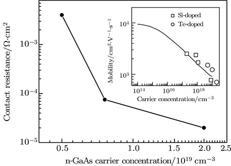
To achieve a good ohmic contact between III–V semiconductor and ITO film, high doping concentrations of both materials are critical and necessary, so that the carriers can tunnel more easily between GaAs and ITO. Therefore, continuous effort to decrease the contacting resistance relies highly on increasing the carrier concentration of GaAs. However, for Si-doped GaAs, when the dopant concentration is higher than , it suffers from a significant self-compensation problem due to the amphoteric dopant nature of Si. Te, however, has been proved to be a perfect n-type dopant for the high electron concentration owing to its low diffusion coefficient and high doping reachability. There are a few reports on Te-doped GaAs. PbTe is usually used as the dopant source.[17] In our study, we chose solid-state elemental Te instead of PbTe as the dopant source because it is environmentally friendly, considering the carcinogenic effect of Pb. The solid-state Te source was loaded into a two-zone thermal cell. The crucible with a small hole on the cap was used for the Te source to enable the accurate control of the dopant flux, which helps to reduce the memory effect significantly. A high carrier concentration of was obtained for GaAs:Te.[17,18] The surface of this highly Te-doped sample was still very smooth because the surfactant effect of Te promotes a smooth surface by enhancing the adatom attachment. The high Te incorporation changed the photoluminescene (PL) behavior of the GaAs film. Figure 2(a) shows the PL spectrum of GaAs:Te. A Gaussian shape was observed. Its PL peak was broadened but symmetric. Compared to the PL peak of the GaAs substrate at 870 nm, the PL peak maximum shifted approximately 110 nm towards higher energy because of the Berstein–Moss shift and the band-shrinkage, which is consistent with the result reported by Jiang desheng et al.[19] In addition, Te has a larger atomic size than arsenic, so it adds a compressive strain to the GaAs substrate. Figure 2(b) shows the XRD spectrum of Te-doped GaAs, the diffraction angle of GaAs:Te is shifted by nearly 0.06° from that of the substrate; but it has little effect on the device performance, since the stress layer is on the top of the whole structure.

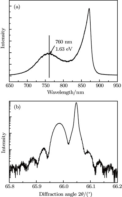
Fig. 2. (a) PL spectrum of GaAs:Te layer with a carrier concentration of 2.5 , (b) the corresponding (004) XRD scans.

Figure 3 presents the contacting resistance of n-GaAs with ITO for different carrier concentrations of n-GaAs. With increasing concentration, the contact resistance decreased. In the case of Te-doped GaAs with the carrier concentration of , the resistance was as low as , which is comparable to that of metal contact. The inset shows the room temperature Hall mobility of n-type GaAs as a function of the carrier concentration. The mobility as a function of the doping density of Te-doped GaAs shows a similar discipline to that of Si-doped GaAs, which indicates that the Te-doped GaAs remains good material quality.

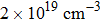
Fig. 3. The contacting resistance of n-GaAs with ITO as a function of the carrier concentration of n-GaAs. The inset shows room temperature RT Hall mobility of n-type GaAs as a function of the carrier concentration.

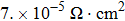
A further study has shown that different annealing conditions have significant effect on the contact resistance. During annealing, the indium, tin, and oxygen diffusions all play important roles in the contact resistance of ITO/GaAs interface. When the carrier concentration of Si-doped GaAs is , the contact resistance of ITO/n-GaAs under different rapid thermal annealing in ambient is given in Fig. 4, which was obtained by a high-precision probe station based on c-TLM method.[16] It can be found that the specific contact resistance decreased with increasing annealed temperature at first, and then increased. With the samples annealed at 480 °C for 3 min, a good ohmic contact between the ITO film and the n-GaAs layer with a low resistivity of was obtained. Under the same annealing condition, the lowest resistance between ITO film and Te-doped GaAs was .

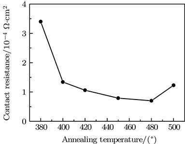
Fig. 4. The contact resistance between ITO and GaAs versus the annealing temperature in ambient .

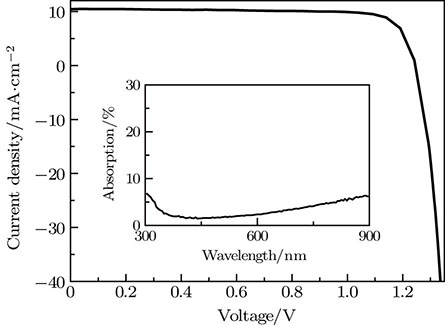
On the basis of the success contact between GaAs and ITO films, a GaInP solar cell with the ITO as the contact layer was fabricated. Figure 5 shows the current density–voltage (JV) characteristics of the GaInP solar cell with the full ITO film electrode under AM1.5G illumination condition. The short-circuit current density ( ), open-circuit voltage ( ), and fill factor (FF) are 10.51 mA/ , 1.24 V, and 80%, respectively, corresponding to a total power conversion efficiency of 10.42%. The lower is due to the imperfect material quality of GaInP as well as its doping.[20] The total photocurrent was lower comparable to our previous reported value in references,[20,21] which is due to the absorption loss of the ITO film and the absence of anti-reflectance film deposition. The inset shows the absorption of pure ITO film. The average absorption loss is less than 5%, corresponding to a current density loss of 0.5 mA/ of the GaInP solar cell. Because of the relatively thin ITO film, the absorption loss of ITO did not have a significant effect on the current density. The main reason is the reflectivity of the ITO film.

Fig. 5. The typical current density–voltage characteristics of the GaInP solar cells with the full ITO film electrode at 1 sun, AM1.5G. The inset shows the absorption of pure ITO film.

The current density was partly benefiting from the nearly zero shadowing loss of the ITO film, the high reflectivity of ITO drives down this positive effect. Figure 6 shows the external quantum efficiency (EQE) of this device. The calculated is about 10 mA/ , which is in good agreement with the measured value from the JV characteristics. The lower EQE is due to the higher surface reflection of the device. Because the ITO film and highly Te-doped GaAs contact layer were direct contacted without ARC layer, the upper surface of the device was covered by pure ITO film. Meanwhile, for the conventional cell, ARC is deposited between the metal fingers. The inset compares the reflectivity of the device with and without ITO. The average reflectivity decreases from 41.0% to 14.5% after employing 100 nm thick ITO film, which indicates that the ITO film could serve as a part of ARC while being used as the electrode. However, even with the ITO deposition, the reflectivity at about 400 nm is still quite high at about 30%. As a result, a very low EQE at around this wavelength range was observed.

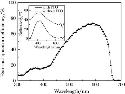
Fig. 6. Quantum efficiency of a GaInP solar cell with the full ITO film electrode structure. The inset shows the reflectivity of the GaInP solar cells with and without depositing the ITO thin film.

A low contact resistance is significantly important to the concentrating application of the device. Figure 6 shows the parameters of the GaInP solar cell with the full ITO electrode under concentration. With increasing concentration, the of the solar cell keeps going up. The device with the full ITO electrode shows a good performance with increasing concentration. This fact indicates that the ITO electrode has a good lateral current expansion. A possible mechanism is that the carriers can easily tunnel across the barrier between the contact layer and the ITO film, because the contact layer is highly doped and thin enough. In the conventional concentration solar cell using metal electrode, in order to decrease the lateral series resistance, we have to increase the thickness of the electrode. In addition, the space of the comb electrode must be smaller than the normal case, i.e., the shadow loss will be increased. However, by using the ITO electrode, carriers were directly collected by the ITO film instead of transportation through metal contact pads. We can reduce the resistance without increasing its thickness and overcome the shadow loss problem in the conventional metal electrode. In addition, the easier fabrication of ITO will be helpful to the future fabrication of large area flexible III–V solar cells. A further study to increase the performance of the ITO-based device will focus on making thinner ITO and combining it with the anti-reflection coating.

Fig. 7. , FF, and efficiency as a function of concentration for the GaInP solar cells with the full ITO film electrode.
4. Conclusion

We successfully applied the pure ITO film as the full front electrode of the GaInP solar cell to replace the conventional bus-bar metal electrode. The lowest contact resistance of
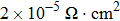
 between ITO and 10 nm -GaAs was obtained. This is benefiting from a highly Te-doped -GaAs layer inserted between ITO and AlInP window layer and a post-growth optimization of thermal annealing. By using the ITO electrode, the resistance could be reduced without increasing its thickness and the shadow loss problem in the conventional metal electrode was avoided. The successful operation of the full ITO electrode not only simplifies the device process, but also gives a great promise to the future application of transparent conducting films in larger area flexible III–V solar cell fabrication.

Reference
[1] King R R Law D C Edmondson K M Fetzer C M Kinsey G S Yoon H Sherif R A Karam N H 2007 Appl. Phys. Lett. 90 183516
[2] King R R Bhusari D Boca A Larrabee D Liu X Q Hong W Fetzer C M Law D C Karam N H 2011 Prog. Photovolt: Res. Appl. 19 797
[3] Guter W Schoene J Philipps S P Sterner M Siefer G Wekkeli A Welser E Oliva E Bett A W Dimroth F 2009 Appl. Phys. Lett. 94 223504
[4] Geisz J F Friedman D J Ward J S Duda A Olavarria W J Moriarty T E Kiehl J T Romero M J Norman A G Jones K M 2007 Appl. Phys. Lett. 91 023502
[5] Li N Lee K Renshaw C K Xiao X Forrest S R 2011 Appl. Phys. Lett. 98 053504
[6] Lai L W Chen J T Lou L R Wu C H Lee C T 2008 J. Electrochem. Soc. 155 B1270
[7] Granqvist C G 2007 Sol. Energy Mater. Sol. Cells 91 1529
[8] Sberveglieri G Comini E Faglia G Ferroni M Jimenez G Vomiero A 2008 In Conference Record of the Thirty Third IEEE Photovoltaic Specialists Conference, San Diego, CA 1 3
[9] Hou J L Wu C H Chang S J 2015 IEEE Electron Device Lett. 36 207
[10] Igasaki Y Kanma H 2001 Appl. Surf. Sci. 169 508
[11] Havard E Camps T Bardinal V Salvagnac L Armand C Fontaine C Pinaud S 2008 Semicond. Sci. Technol. 23 035001
[12] Tseng C Y Lee C T 2013 Sol. Energy 89 17
[13] Tseng C Y Lee C K Lee C T 2011 Prog. Photovolt: Res. Appl. 19 436
[14] Cheng C W Shiu K T Li N Han S J Shi L Sadana D K 2013 Nat. Commun. 4 67
[15] Kayes B M Zhang L Twist R Ding I K Higashi G S 2014 IEEE J. Photovoltaics 4 729
[16] Ho J K Jong C S Chiu C C Huang C N Shih K K Chen L C Chen R F Kai J J 1999 J. Appl. Phys. 86 4491
[17] Dai P Tan M Wu Y Y Ji L Bian L F Lu S L Yang H 2015 J. Crystal Growth 413 71
[18] Gan X Y Zheng X H Wu Y Y Lu S L Yang H Arimochi M Watanabe T Ikeda M Nomachi I Yoshida H Uchida S 2014 Jpn. J. Appl. Phys. 53 021201
[19] Jiang D S Makita Y Ploog K Queisser H J 1982 J. Appl. Phys. 53 999
[20] Dai P Lu S L Arimochi M Uchida S Watanabe T Luo X D Yang H 2014 Solid State Commu. 200 9
[21] Lu S L Ji L He W Dai P Yang H Arimochi M Yoshida H Uchida S Ikeda M 2011 Nanos. Res. Lett. 6 576