Band gap engineering of atomically thin two-dimensional semiconductors
Project supported by the National Natural Science Foundation of China (Grant Nos. 11374092, 61474040, 61574054, and 61505051), the Aid Program for Science and Technology Innovative Research Team in Higher Educational Institutions of Hunan Province, China, and the Science and Technology Department of Hunan Province, China (Grant No. 2014FJ2001).
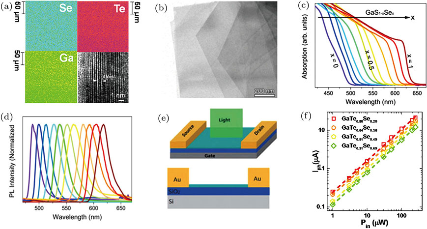
(color online) (a) EDX mapping of Se, Te, and Ga in a GaTe